IRFB4332PBF International Rectifier, IRFB4332PBF Datasheet - Page 2
IRFB4332PBF
Manufacturer Part Number
IRFB4332PBF
Description
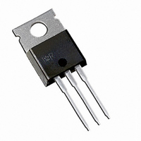
MOSFET N-CH 250V 60A TO-220AB
Manufacturer
International Rectifier
Series
HEXFET®r
Datasheet
1.IRFB4332PBF.pdf
(8 pages)
Specifications of IRFB4332PBF
Fet Type
MOSFET N-Channel, Metal Oxide
Fet Feature
Standard
Rds On (max) @ Id, Vgs
33 mOhm @ 35A, 10V
Drain To Source Voltage (vdss)
250V
Current - Continuous Drain (id) @ 25° C
60A
Vgs(th) (max) @ Id
5V @ 250µA
Gate Charge (qg) @ Vgs
150nC @ 10V
Input Capacitance (ciss) @ Vds
5860pF @ 25V
Power - Max
390W
Mounting Type
Through Hole
Package / Case
TO-220-3 (Straight Leads)
Transistor Polarity
N-Channel
Drain-source Breakdown Voltage
250 V
Gate-source Breakdown Voltage
30 V
Continuous Drain Current
60 A
Power Dissipation
390 W
Mounting Style
Through Hole
Gate Charge Qg
99 nC
Lead Free Status / RoHS Status
Lead free / RoHS Compliant
Available stocks
Company
Part Number
Manufacturer
Quantity
Price
Company:

Part Number:
IRFB4332PBF
Manufacturer:
MTK
Quantity:
101
Part Number:
IRFB4332PBF
Manufacturer:
IR
Quantity:
20 000


BV
ΔΒV
R
V
ΔV
I
I
g
Q
Q
t
E
C
C
C
C
L
L
E
E
V
I
I
I
V
t
Q
IRFB4332PbF
Electrical Characteristics @ T
Avalanche Characteristics
Diode Characteristics
DSS
GSS
st
AS
S
SM
rr
fs
D
S
DS(on)
GS(th)
PULSE
iss
oss
rss
oss
AS
AR
DS(Avalanche)
SD
g
gd
rr
@ T
2
GS(th)
DSS
DSS
eff.
C
/ΔT
/ΔT
= 25°C Continuous Source Current
J
J
Drain-to-Source Breakdown Voltage
Breakdown Voltage Temp. Coefficient
Static Drain-to-Source On-Resistance
Gate Threshold Voltage
Gate Threshold Voltage Coefficient
Drain-to-Source Leakage Current
Gate-to-Source Forward Leakage
Gate-to-Source Reverse Leakage
Forward Transconductance
Total Gate Charge
Gate-to-Drain Charge
Shoot Through Blocking Time
Energy per Pulse
Input Capacitance
Output Capacitance
Reverse Transfer Capacitance
Effective Output Capacitance
Internal Drain Inductance
Internal Source Inductance
Single Pulse Avalanche Energyd
Repetitive Avalanche Energy c
Repetitive Avalanche Voltage c
Avalanche Current d
(Body Diode)
Pulsed Source Current
(Body Diode) c
Diode Forward Voltage
Reverse Recovery Time
Reverse Recovery Charge
Parameter
Parameter
Parameter
J
= 25°C (unless otherwise specified)
Min. Typ. Max. Units
Min. Typ. Max. Units
250
–––
–––
–––
–––
–––
–––
–––
100
–––
–––
100
–––
–––
–––
–––
–––
–––
–––
–––
–––
–––
–––
–––
–––
3.0
5860
–––
170
–––
–––
–––
–––
–––
–––
–––
520
920
530
130
360
–––
–––
–––
190
820
-14
4.5
7.5
29
99
35
1230
-100
Typ.
–––
–––
–––
–––
–––
100
–––
150
–––
–––
–––
–––
–––
–––
–––
–––
–––
–––
300
–––
230
290
5.0
1.0
1.3
33
20
60
mV/°C
mV/°C
mΩ
mA
μA
nA
nC
nH
nC
pF
ns
μJ
ns
V
V
S
A
V
V
Reference to 25°C, I
V
V
V
V
V
V
V
V
V
L = 220nH, C= 0.3μF, V
V
L = 220nH, C= 0.3μF, V
V
V
V
ƒ = 1.0MHz,
V
Between lead,
6mm (0.25in.)
from package
and center of die contact
MOSFET symbol
showing the
integral reverse
p-n junction diode.
T
T
di/dt = 100A/μs e
J
J
GS
GS
DS
DS
DS
GS
GS
DS
DD
DD
DS
DS
GS
DS
GS
= 25°C, I
= 25°C, I
= V
= 250V, V
= 250V, V
= 25V, I
= 200V, R
= 200V, R
= 25V
= 0V, I
= 10V, I
= 20V
= -20V
= 125V, I
= 200V, V
= 0V
= 0V, V
GS
Max.
230
–––
39
35
, I
D
S
F
D
DS
Conditions
D
Conditions
D
= 250μA
= 35A, V
= 35A, V
= 250μA
D
= 35A e
= 35A
GS
GS
GS
G
G
= 0V to 200V
= 35A, V
= 5.1Ω, T
= 5.1Ω, T
= 0V
= 0V, T
= 15V, R
D
GS
DD
= 1mA
www.irf.com
GS
J
GS
GS
= 0V e
= 50V
J
J
= 125°C
G
= 10Ve
Units
= 25°C
= 100°C
= 4.7Ω
= 15V
= 15V
mJ
mJ
V
A
G
S
D
Related parts for IRFB4332PBF
Image
Part Number
Description
Manufacturer
Datasheet
Request
R

Part Number:
Description:
SCHOTTKY RECTIFIER
Manufacturer:
International Rectifier Corp.
Datasheet:
Part Number:
Description:
SCHOTTKY RECTIFIER
Manufacturer:
International Rectifier Corp.
Datasheet:
Part Number:
Description:
SCHOTTKY RECTIFIER
Manufacturer:
International Rectifier Corp.
Datasheet:
Part Number:
Description:
SCHOTTKY RECTIFIER
Manufacturer:
International Rectifier Corp.
Datasheet:
Part Number:
Description:
SCHOTTKY RECTIFIER
Manufacturer:
International Rectifier Corp.
Datasheet:
Part Number:
Description:
SCHOTTKY RECTIFIER
Manufacturer:
International Rectifier Corp.
Datasheet:
Part Number:
Description:
SCHOTTKY RECTIFIER
Manufacturer:
International Rectifier Corp.
Datasheet:
Part Number:
Description:
SCHOTTKY RECTIFIER
Manufacturer:
International Rectifier Corp.
Datasheet:
Part Number:
Description:
SCHOTTKY RECTIFIER
Manufacturer:
International Rectifier Corp.
Datasheet:
Part Number:
Description:
SCHOTTKY RECTIFIER
Manufacturer:
International Rectifier Corp.
Datasheet:
Part Number:
Description:
SCHOTTKY RECTIFIER
Manufacturer:
International Rectifier Corp.
Datasheet:
Part Number:
Description:
SCHOTTKY RECTIFIER
Manufacturer:
International Rectifier Corp.
Datasheet:
Part Number:
Description:
SCHOTTKY RECTIFIER
Manufacturer:
International Rectifier Corp.
Datasheet:
Part Number:
Description:
SCHOTTKY RECTIFIER
Manufacturer:
International Rectifier Corp.
Datasheet:
Part Number:
Description:
SCHOTTKY RECTIFIER
Manufacturer:
International Rectifier Corp.
Datasheet: