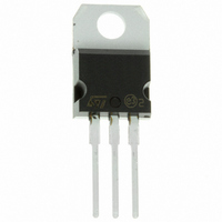
IRF520 STMicroelectronics, IRF520 Datasheet - Page 3

IRF520
Manufacturer Part Number
IRF520
Description
MOSFET N-CH 100V 10A TO-220
Manufacturer
STMicroelectronics
Series
STripFET™r
Datasheet
1.IRF520.pdf
(8 pages)
Specifications of IRF520
Fet Type
MOSFET N-Channel, Metal Oxide
Fet Feature
Logic Level Gate
Rds On (max) @ Id, Vgs
270 mOhm @ 7A, 10V
Drain To Source Voltage (vdss)
100V
Current - Continuous Drain (id) @ 25° C
10A
Vgs(th) (max) @ Id
4V @ 250µA
Gate Charge (qg) @ Vgs
22nC @ 10V
Input Capacitance (ciss) @ Vds
460pF @ 25V
Power - Max
60W
Mounting Type
Through Hole
Package / Case
TO-220-3 (Straight Leads)
Lead Free Status / RoHS Status
Contains lead / RoHS non-compliant
Other names
497-2782-5
Available stocks
Company
Part Number
Manufacturer
Quantity
Price
Part Number:
IRF520
Manufacturer:
IR
Quantity:
20 000
Company:
Part Number:
IRF520A
Manufacturer:
IR
Quantity:
12 500
Company:
Part Number:
IRF520FI
Manufacturer:
ST
Quantity:
10 000
Company:
Part Number:
IRF520FI
Manufacturer:
IR
Quantity:
12 500
Company:
Part Number:
IRF520L
Manufacturer:
IR
Quantity:
12 500
Part Number:
IRF520NPBF
Manufacturer:
IR
Quantity:
20 000
ELECTRICAL CHARACTERISTICS (continued)
SWITCHING ON
SWITCHING OFF
SOURCE DRAIN DIODE
(*)
(
Safe Operating Area
Pulsed: Pulse duration = 300 µs, duty cycle 1.5 %.
Pulse width limited by safe operating area.
Symbol
Symbol
Symbol
I
V
SDM
t
t
I
Q
d(on)
Q
d(off)
SD
RRM
I
Q
Q
SD
t
t
t
rr
gs
gd
r
f
rr
g
(*)
( )
Turn-on Delay Time
Rise Time
Total Gate Charge
Gate-Source Charge
Gate-Drain Charge
Turn-off Delay Time
Fall Time
Source-drain Current
Source-drain Current (pulsed)
Forward On Voltage
Reverse Recovery Time
Reverse Recovery Charge
Reverse Recovery Current
Parameter
Parameter
Parameter
V
(Resistive Load, Figure 3)
V
V
R
(Resistive Load, Figure 3)
I
I
V
(see test circuit, Figure 5)
SD
SD
R
DD
DD
DD
DD
G
G
= 4.7
= 10 A
= 10 A
= 50 V
= 80V I
= 50 V
= 40V
= 4.7
Test Conditions
Test Conditions
Test Conditions
D
= 10A V
Thermal Impedance
di/dt = 100A/µs
V
V
GS
T
GS
j
V
I
= 150°C
D
= 10 V
GS
I
D
GS
= 7 A
= 0
= 7 A
= 10 V
= 10V
Min.
Min.
Min.
Typ.
Typ.
Typ.
230
16
25
16
32
95
4
5
8
5
Max.
Max.
Max.
1.5
22
10
40
IRF520
Unit
Unit
Unit
nC
nC
nC
nC
ns
ns
ns
ns
ns
A
A
V
A
3/8


