BSL307SP Infineon Technologies, BSL307SP Datasheet - Page 2
BSL307SP
Manufacturer Part Number
BSL307SP
Description
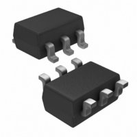
MOSFET P-CH 30V 5.5A 6-TSOP
Manufacturer
Infineon Technologies
Series
OptiMOS™r
Datasheet
1.BSL307SP.pdf
(8 pages)
Specifications of BSL307SP
Fet Type
MOSFET P-Channel, Metal Oxide
Fet Feature
Logic Level Gate
Rds On (max) @ Id, Vgs
43 mOhm @ 5.5A, 10V
Drain To Source Voltage (vdss)
30V
Current - Continuous Drain (id) @ 25° C
5.5A
Vgs(th) (max) @ Id
2V @ 40µA
Gate Charge (qg) @ Vgs
29nC @ 10V
Input Capacitance (ciss) @ Vds
805pF @ 25V
Power - Max
2W
Mounting Type
Surface Mount
Package / Case
6-TSOP
Package
TSOP-6
Vds (max)
-30.0 V
Rds (on) (max) (@10v)
43.0 mOhm
Rds (on) (max) (@4.5v)
74.0 mOhm
Rds (on) (max) (@2.5v)
-
Lead Free Status / RoHS Status
Contains lead / RoHS non-compliant
Other names
BSL307SPINTR
Available stocks
Company
Part Number
Manufacturer
Quantity
Price
Company:

Part Number:
BSL307SP
Manufacturer:
Infineon
Quantity:
98 000
Part Number:
BSL307SP
Manufacturer:
INFINEON/英飞凌
Quantity:
20 000
Company:
Part Number:
BSL307SP L6327
Manufacturer:
Infineon Technologies
Quantity:
31 450
Company:
Part Number:
BSL307SP L6327
Manufacturer:
Infineon
Quantity:
20 000
Part Number:
BSL307SP L6327
Manufacturer:
INFINEON/英飞凌
Quantity:
20 000
Part Number:
BSL307SPH6327
Manufacturer:
INFINEON/英飞凌
Quantity:
20 000


Electrical Characteristics, at T
Parameter
Static Characteristics
Drain-source breakdown voltage
V
Gate threshold voltage, V
I
Zero gate voltage drain current
V
V
Gate-source leakage current
V
Drain-source on-state resistance
V
Drain-source on-state resistance
V
1 Device on 40mm*40mm*1.5mm epoxy PCB FR4 with 6cm 2 (one layer, 70 µm thick) copper area for drain
connection. PCB is vertical without blown air; t 5 sec.
Thermal Characteristics
Parameter
Characteristics
Thermal resistance, junction - soldering point
SMD version, device on PCB:
@ min. footprint
@ 6 cm
D
GS
DS
DS
GS
GS
GS
=-40µA
=-30V, V
=-30V, V
=0, I
=-20V, V
=-4.5V, I
=-10V, I
2
D
cooling area
=-250µA
D
GS
GS
D
DS
=-5.5A
=-4.2A
=0, T
=0, T
=0
j
j
=25°C
=150°C
1)
GS
= V
j
DS
= 25 °C, unless otherwise specified
Rev 1.2
Page 2
Symbol
V
V
I
I
R
R
Symbol
R
R
DSS
GSS
(BR)DSS
GS(th)
DS(on)
DS(on)
thJS
thJA
min.
min.
-30
-1
-
-
-
-
-
-
-
-
Values
Values
-0.1
typ.
-1.5
-10
typ.
-10
52
31
-
-
-
-
max.
max.
-100
-100
62.5
230
BSL307SP
74
43
50
2007-02-23
-2
-1
-
Unit
V
µA
nA
m
Unit
K/W
Related parts for BSL307SP
Image
Part Number
Description
Manufacturer
Datasheet
Request
R

Part Number:
Description:
Manufacturer:
Infineon Technologies AG
Datasheet:
Part Number:
Description:
Manufacturer:
Infineon Technologies AG
Datasheet:
Part Number:
Description:
Manufacturer:
Infineon Technologies AG
Datasheet:
Part Number:
Description:
Manufacturer:
Infineon Technologies AG
Datasheet:
Part Number:
Description:
Manufacturer:
Infineon Technologies AG
Datasheet:
Part Number:
Description:
Manufacturer:
Infineon Technologies AG
Datasheet:
Part Number:
Description:
Manufacturer:
Infineon Technologies AG
Datasheet:
Part Number:
Description:
16-bit microcontroller with 2x2 KByte RAM
Manufacturer:
Infineon Technologies AG
Datasheet:
Part Number:
Description:
NPN silicon RF transistor
Manufacturer:
Infineon Technologies AG
Datasheet:
Part Number:
Description:
NPN silicon RF transistor
Manufacturer:
Infineon Technologies AG
Datasheet:
Part Number:
Description:
NPN silicon RF transistor
Manufacturer:
Infineon Technologies AG
Datasheet:
Part Number:
Description:
NPN silicon RF transistor
Manufacturer:
Infineon Technologies AG
Datasheet:
Part Number:
Description:
Si-MMIC-amplifier in SIEGET 25-technologie
Manufacturer:
Infineon Technologies AG
Datasheet:
Part Number:
Description:
IGBT Power Module
Manufacturer:
Infineon Technologies AG
Datasheet:
Part Number:
Description:
IC for switching-mode power supplies
Manufacturer:
Infineon Technologies AG
Datasheet: