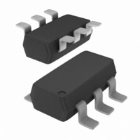
PBLS2024D,115 NXP Semiconductors, PBLS2024D,115 Datasheet - Page 13

PBLS2024D,115
Manufacturer Part Number
PBLS2024D,115
Description
LOADSWITCH PNP 1.8A 20V SOT457
Manufacturer
NXP Semiconductors
Datasheet
1.PBLS2024D115.pdf
(16 pages)
Specifications of PBLS2024D,115
Package / Case
SC-74-6
Transistor Type
1 NPN Pre-Biased, 1 PNP
Current - Collector (ic) (max)
100mA, 1.8A
Voltage - Collector Emitter Breakdown (max)
50V, 20V
Resistor - Base (r1) (ohms)
22K
Resistor - Emitter Base (r2) (ohms)
22K
Dc Current Gain (hfe) (min) @ Ic, Vce
60 @ 5mA, 5V / 200 @ 1A, 2V
Vce Saturation (max) @ Ib, Ic
150mV @ 500µA, 10mA / 210mV @ 100mA, 1.8A
Current - Collector Cutoff (max)
1µA, 100nA
Frequency - Transition
130MHz
Power - Max
760mW
Mounting Type
Surface Mount
Configuration
Dual
Transistor Polarity
PNP
Typical Input Resistor
22 KOhms
Typical Resistor Ratio
1
Mounting Style
SMD/SMT
Collector- Emitter Voltage Vceo Max
- 20 V
Continuous Collector Current
- 1.8 A
Peak Dc Collector Current
- 3 A
Power Dissipation
370 mW
Maximum Operating Temperature
+ 150 C
Emitter- Base Voltage Vebo
- 5 V
Minimum Operating Temperature
- 55 C
Lead Free Status / RoHS Status
Lead free / RoHS Compliant
Other names
934061576115
NXP Semiconductors
9. Package outline
10. Packing information
PBLS2024D_2
Product data sheet
Table 8.
The indicated -xxx are the last three digits of the 12NC ordering code.
[1]
[2]
[3]
Type number Package Description
PBLS2024D
Fig 20. Package outline SOT457 (SC-74)
For further information and the availability of packing methods, see
T1: normal taping
T2: reverse taping
Packing methods
SOT457
3.0
2.5
Rev. 02 — 6 September 2009
Dimensions in mm
1.7
1.3
4 mm pitch, 8 mm tape and reel; T1
4 mm pitch, 8 mm tape and reel; T2
pin 1 index
1
6
0.95
3.1
2.7
1.9
5
2
4
3
0.40
0.25
20 V, 1.8 A PNP BISS loadswitch
0.6
0.2
Section
[1]
1.1
0.9
0.26
0.10
PBLS2024D
04-11-08
13.
[2]
[3]
Packing quantity
3000
-115
-125
© NXP B.V. 2009. All rights reserved.
10000
-135
-165
13 of 16


