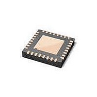
ISP1504CBS NXP Semiconductors, ISP1504CBS Datasheet - Page 13

ISP1504CBS
Manufacturer Part Number
ISP1504CBS
Description
RF Transceiver USB2.0 ULPI OTG TRANSCEIVER
Manufacturer
NXP Semiconductors
Datasheet
1.ISP1504ABS118.pdf
(83 pages)
Specifications of ISP1504CBS
Operating Supply Voltage
1.65 V to 3.6 V
Mounting Style
SMD/SMT
Package / Case
HVQFN
Minimum Operating Temperature
- 40 C
Lead Free Status / RoHS Status
Lead free / RoHS Compliant
Other names
ISP1504CBS,157
Available stocks
Company
Part Number
Manufacturer
Quantity
Price
Part Number:
ISP1504CBS
Manufacturer:
NXP/恩智浦
Quantity:
20 000
Company:
Part Number:
ISP1504CBSFA
Manufacturer:
NXP
Quantity:
6 041
NXP Semiconductors
ISP1504A_ISP1504C_3
Product data sheet
7.9.10 PSW_N
7.9.11 V
7.9.8 C_A and C_B
7.9.9 V
The C_A and C_B pins are to connect the flying capacitor of the charge pump. The output
current capability of the charge pump depends on the value of the capacitor used, as
shown in
For details, see
If the charge pump is not used, C_A and C_B must be left floating (not connected).
Table 3.
V
recommended. For details, see
PSW_N is an active LOW, open-drain output pin. This pin can be connected to an active
LOW, external V
power source. An external pull-up resistor, R
pin is open-drain, allowing ganged-mode power control for multiple USB ports. For
application details, see
If the link is in host mode, it can enable the external V
DRV_VBUS_EXT bit in the OTG Control register to logic 1. The ISP1504 will drive
PSW_N to LOW to enable the external V
overcurrent condition (the V
V
This pin acts as an input to V
pump, and SRP charge and discharge resistors.
When the DRV_VBUS bit of the OTG Control register is set to logic 1, the ISP1504 drives
V
The V
C
22 nF
270 nF
Fig 4.
CC
BUS
BUS
CC
BUS
cp(C_A)-(C_B)
is the main input supply voltage for the ISP1504. Decoupling capacitors are
power source by setting DRV_VBUS_EXT to logic 0.
to a voltage of 4.4 V to 5.25 V, with a minimum output current capability of 8 mA.
BUS
Table
Charge pump capacitor
pin requires a capacitive load as shown in
Recommended charge pump capacitor value
3. For maximum efficiency, place capacitors as close as possible to pins.
Section
BUS
switch or charge pump enable circuit to control the external V
Section
Rev. 03 — 7 April 2008
16.
BUS
BUS
ISP1504
Section
16.
state in RXCMD is not 11b), it must disable the external
comparators, and also as a power pin for the charge
C_A
C_B
16.
V
BUS
BUS
pullup
power source. If the link detects an
004aaa516
I
8 mA
50 mA
ISP1504A; ISP1504C
L
(max)
, is required when PSW_N is used. This
C cp(C_A)-(C_B)
Section
I L
BUS
ULPI HS USB OTG transceiver
power source by setting the
16.
© NXP B.V. 2008. All rights reserved.
BUS
12 of 82


