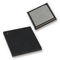
PIC18F65K90T-I/MR Microchip Technology, PIC18F65K90T-I/MR Datasheet - Page 231

PIC18F65K90T-I/MR
Manufacturer Part Number
PIC18F65K90T-I/MR
Description
32kB Flash, 2kB RAM, 1kB EE, NanoWatt XLP, LCD 64 QFN 9x9x0.9mm T/R
Manufacturer
Microchip Technology
Series
PIC® XLP™ 18Fr
Datasheet
1.PIC18F66K90-IMR.pdf
(570 pages)
Specifications of PIC18F65K90T-I/MR
Processor Series
PIC18F
Core
PIC
Data Bus Width
8 bit
Program Memory Type
Flash
Program Memory Size
32 KB
Data Ram Size
2 KB
Interface Type
I2C, SPI
Maximum Clock Frequency
64 MHz
Number Of Timers
8
Operating Supply Voltage
1.8 V to 5.5 V
Maximum Operating Temperature
+ 125 C
3rd Party Development Tools
52715-96, 52716-328, 52717-734, 52712-325, EWPIC18
Minimum Operating Temperature
- 40 C
On-chip Adc
12 bit, 16 Channel
Core Processor
PIC
Core Size
8-Bit
Speed
64MHz
Connectivity
I²C, LIN, SPI, UART/USART
Peripherals
Brown-out Detect/Reset, LCD, POR, PWM, WDT
Number Of I /o
53
Eeprom Size
1K x 8
Ram Size
2K x 8
Voltage - Supply (vcc/vdd)
1.8 V ~ 5.5 V
Data Converters
A/D 16x12b
Oscillator Type
Internal
Operating Temperature
-40°C ~ 85°C
Package / Case
64-VFQFN Exposed Pad
Lead Free Status / Rohs Status
Details
- Current page: 231 of 570
- Download datasheet (5Mb)
17.2.4
Since the year range on the RTCC module is 2000 to
2099, the leap year calculation is determined by any year
divisible by four in the above range. Only February is
affected in a leap year.
February will have 29 days in a leap year and 28 days in
any other year.
17.2.5
All Timer registers containing a time value of seconds or
greater are writable. The user configures the time by
writing the required year, month, day, hour, minutes and
seconds to the Timer registers, via Register Pointers.
(See
The timer uses the newly written values and proceeds
with the count from the required starting point.
The RTCC is enabled by setting the RTCEN bit
(RTCCFG<7>). If enabled, while adjusting these regis-
ters, the timer still continues to increment. However, any
time the MINSEC register is written to, both of the timer
prescalers are reset to ‘0’. This allows fraction of a
second synchronization.
The Timer registers are updated in the same cycle as
the write instruction’s execution by the CPU. The user
must ensure that when RTCEN = 1, the updated
registers will not be incremented at the same time. This
can be accomplished in several ways:
• By checking the RTCSYNC bit (RTCCFG<4>)
• By checking the preceding digits from which a
• By updating the registers immediately following
The user has visibility to the half-second field of the
counter. This value is read-only and can be reset only
by writing to the lower half of the SECONDS register.
17.2.6
The RTCSYNC bit indicates a time window during
which the RTCC Clock Domain registers can be safely
read and written without concern about a rollover.
When RTCSYNC = 0, the registers can be safely
accessed by the CPU.
Whether RTCSYNC = 1 or 0, the user should employ a
firmware solution to ensure that the data read did not
fall on a rollover boundary, resulting in an invalid or
partial read. This firmware solution would consist of
reading each register twice and then comparing the two
values. If the two values matched, then a rollover did
not occur.
2009-2011 Microchip Technology Inc.
carry can occur
the seconds pulse (or an alarm interrupt)
Section 17.2.8 “Register
LEAP YEAR
GENERAL FUNCTIONALITY
SAFETY WINDOW FOR REGISTER
READS AND WRITES
Mapping”.)
PIC18F87K90 FAMILY
17.2.7
In order to perform a write to any of the RTCC Timer
registers, the RTCWREN bit (RTCCFG<5>) must be set.
To avoid accidental writes to the RTCC Timer register,
it
(RTCCFG<5>) be kept clear when not writing to the
register. For the RTCWREN bit to be set, there is only
one instruction cycle time window allowed between the
55h/AA sequence and the setting of RTCWREN. For
that reason, it is recommended that users follow the
code example in
EXAMPLE 17-1:
17.2.8
To limit the register interface, the RTCC Timer and
Alarm
corresponding Register Pointers. The RTCC Value
register window (RTCVALH and RTCVALL) uses the
RTCPTRx bits (RTCCFG<1:0>) to select the required
Timer register pair.
By reading or writing to the RTCVALH register, the
RTCC Pointer value (RTCPTR<1:0>) decrements by ‘1’
until it reaches ‘00’. When ‘00’ is reached, the
MINUTES and SECONDS value is accessible through
RTCVALH and RTCVALL until the pointer value is
manually changed.
TABLE 17-3:
The Alarm Value register windows (ALRMVALH and
ALRMVALL) use the ALRMPTR bits (ALRMCFG<1:0>)
to select the desired alarm register pair.
By reading or writing to the ALRMVALH register, the
Alarm Pointer value, ALRMPTR<1:0>, decrements by
one until it reaches ‘00’. When it reaches ‘00’, the
ALRMMIN and ALRMSEC value is accessible through
ALRMVALH and ALRMVALL until the pointer value is
manually changed.
RTCPTR<1:0>
is
movlw
movwf
movlw
movwf
bsf
00
01
10
11
recommended
Timer
WRITE LOCK
REGISTER MAPPING
registers
Example
RTCVALH AND RTCVALL
REGISTER MAPPING
0x55
EECON2
0xAA
EECON2
RTCCFG,RTCWREN
RTCC Value Register Window
WEEKDAY
RTCVALH
MINUTES
SETTING THE
RTCWREN BIT
MONTH
that
—
17-1.
are
the
accessed
DS39957D-page 231
RTCWREN
SECONDS
RTCVALL
HOURS
YEAR
DAY
through
bit
Related parts for PIC18F65K90T-I/MR
Image
Part Number
Description
Manufacturer
Datasheet
Request
R

Part Number:
Description:
Manufacturer:
Microchip Technology Inc.
Datasheet:

Part Number:
Description:
Manufacturer:
Microchip Technology Inc.
Datasheet:

Part Number:
Description:
Manufacturer:
Microchip Technology Inc.
Datasheet:

Part Number:
Description:
Manufacturer:
Microchip Technology Inc.
Datasheet:

Part Number:
Description:
Manufacturer:
Microchip Technology Inc.
Datasheet:

Part Number:
Description:
Manufacturer:
Microchip Technology Inc.
Datasheet:

Part Number:
Description:
Manufacturer:
Microchip Technology Inc.
Datasheet:

Part Number:
Description:
Manufacturer:
Microchip Technology Inc.
Datasheet:


