PIC18F65K90T-I/MR Microchip Technology, PIC18F65K90T-I/MR Datasheet - Page 560
PIC18F65K90T-I/MR
Manufacturer Part Number
PIC18F65K90T-I/MR
Description
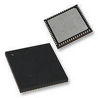
32kB Flash, 2kB RAM, 1kB EE, NanoWatt XLP, LCD 64 QFN 9x9x0.9mm T/R
Manufacturer
Microchip Technology
Series
PIC® XLP™ 18Fr
Datasheet
1.PIC18F66K90-IMR.pdf
(570 pages)
Specifications of PIC18F65K90T-I/MR
Processor Series
PIC18F
Core
PIC
Data Bus Width
8 bit
Program Memory Type
Flash
Program Memory Size
32 KB
Data Ram Size
2 KB
Interface Type
I2C, SPI
Maximum Clock Frequency
64 MHz
Number Of Timers
8
Operating Supply Voltage
1.8 V to 5.5 V
Maximum Operating Temperature
+ 125 C
3rd Party Development Tools
52715-96, 52716-328, 52717-734, 52712-325, EWPIC18
Minimum Operating Temperature
- 40 C
On-chip Adc
12 bit, 16 Channel
Core Processor
PIC
Core Size
8-Bit
Speed
64MHz
Connectivity
I²C, LIN, SPI, UART/USART
Peripherals
Brown-out Detect/Reset, LCD, POR, PWM, WDT
Number Of I /o
53
Eeprom Size
1K x 8
Ram Size
2K x 8
Voltage - Supply (vcc/vdd)
1.8 V ~ 5.5 V
Data Converters
A/D 16x12b
Oscillator Type
Internal
Operating Temperature
-40°C ~ 85°C
Package / Case
64-VFQFN Exposed Pad
Lead Free Status / Rohs Status
Details


PIC18F87K90 FAMILY
LCD Driver .......................................................................... 10
LCDCON Register............................................................. 274
LCDDATAx Registers ....................................................... 274
LCDPS Register................................................................ 274
LCDSEx Registers ............................................................ 274
LFSR ................................................................................. 475
Liquid Crystal Display (LCD) Driver .................................. 273
M
Master Clear (MCLR) .......................................................... 71
Master Synchronous Serial Port (MSSP). See MSSP.
Memory Organization.......................................................... 85
Microchip Internet Web Site .............................................. 566
Migration From PIC18F85J90 and
MOVF................................................................................ 475
MOVFF.............................................................................. 476
MOVLB.............................................................................. 476
MOVLW............................................................................. 477
MOVSF ............................................................................. 495
MOVSS ............................................................................. 496
MOVWF ............................................................................ 477
MPLAB ASM30 Assembler, Linker, Librarian ................... 502
MPLAB Integrated Development Environment
MPLAB PM3 Device Programmer..................................... 504
MPLAB REAL ICE In-Circuit Emulator System................. 503
MPLINK Object Linker/MPLIB Object Librarian ................ 502
MSSP
MULLW ............................................................................. 478
MULWF ............................................................................. 478
DS39957D-page 560
Operation During Sleep ............................................ 299
Pixel Control.............................................................. 285
Prescaler ................................................................... 280
Segment Enables...................................................... 285
Waveform Generation ............................................... 286
LP3:LP0 Bits ............................................................. 280
Data Memory .............................................................. 92
Program Memory
PIC18F87J90 to PIC18F87K90 ................................ 553
Software .................................................................... 501
ACK Pulse......................................................... 318, 321
I
Module Overview ...................................................... 303
SPI Mode .................................................................. 303
SPI Mode Serial Data In ........................................... 303
2
C Mode. See I
Memory Maps ..................................................... 85
Associated Registers ........................................ 312
Bus Mode Compatibility .................................... 311
Clock Speed, Interactions ................................. 311
Effects of a Reset.............................................. 311
Enabling SPI I/O ............................................... 307
Master Mode ..................................................... 308
Operation .......................................................... 306
Operation in Power-Managed Modes ............... 311
Serial Clock....................................................... 303
Serial Data Out ................................................. 303
Slave Mode ....................................................... 309
Slave Select ...................................................... 303
Slave Select Synchronization ........................... 309
SPI Clock .......................................................... 308
SSPxBUF Register ........................................... 308
SSPxSR Register.............................................. 308
Typical Connection ........................................... 307
2
C Mode.
N
NEGF................................................................................ 479
NOP .................................................................................. 479
Notable Differences Between PIC18F87K90,
O
On-Chip Regulator............................................................ 425
On-Chip Voltage Regulator............................................... 442
Oscillator Configuration ...................................................... 41
Oscillator Selection ........................................................... 425
Oscillator Start-up Timer (OST) .......................................... 52
Oscillator, Timer1.............................................................. 187
P
P1A/P1B/P1C/P1D. See Enhanced
Packaging ......................................................................... 545
Pin Functions
PIC18F87J90 and PIC18F85J90 Families ............... 554
Enable/Disable by Hardware .................................... 442
Clock Sources, Switching ........................................... 45
EC............................................................................... 41
ECIO ........................................................................... 41
HS............................................................................... 41
Internal Oscillator Block .............................................. 49
INTIO1 ........................................................................ 41
INTIO2 ........................................................................ 41
LP ............................................................................... 41
RC .............................................................................. 41
RCIO........................................................................... 41
Transitions .................................................................. 46
XT ............................................................................... 41
Capture/Compare/PWM (ECCP). ............................. 257
Details....................................................................... 546
Marking ..................................................................... 545
AV
AV
ENVREG .............................................................. 22, 33
MCLR/RG5 ........................................................... 14, 22
OSC1/CLKI/RA7 ................................................... 14, 22
OSC2/CLKO/RA6 ................................................. 14, 22
RA0/AN0/ULPWU................................................. 15, 23
RA1/AN1/SEG18 .................................................. 15, 23
RA2/AN2/V
RA3/AN3/
RA3/AN3/V
RA4/T0CKI/SEG14 ............................................... 15, 23
RA5/AN4/SEG15/T1CKI/T3G/HLVDIN................. 15, 23
RB0/INT0/SEG30/FLT0 .............................................. 24
RB0/INT0/SEG30/FLTO ............................................. 16
RB1/INT1/SEG8 ................................................... 16, 24
RB2/INT2/SEG9/CTED1....................................... 16, 24
RB3/INT3/SEG10/CTED2/ECCP2/P2A................ 16, 24
RB4/KBI0/SEG11 ................................................. 16, 24
RB5/KBI1/SEG29/T3CKI/T1G .............................. 16, 24
RB6/KBI2/PGC ..................................................... 16, 25
RB7/KBI3/PGD ..................................................... 16, 25
RC0/SOSCO/SCKLI ................................................... 26
RC0/SOSCO/SCLKI ................................................... 17
RC1/SOSCI/ECCP2/P2A/SEG32 ............................... 17
RC1/SOSCI/ECCP2/SEG32/P2A ............................... 26
RC2/ECCP1/P1A/SEG13 ..................................... 17, 26
DD
SS
..................................................................... 22, 33
..................................................................... 22, 33
REF
REF
REF
+............................................................ 15
- .................................................... 15, 23
+ ......................................................... 23
2009-2011 Microchip Technology Inc.
Related parts for PIC18F65K90T-I/MR
Image
Part Number
Description
Manufacturer
Datasheet
Request
R

Part Number:
Description:
Manufacturer:
Microchip Technology Inc.
Datasheet:
Part Number:
Description:
Manufacturer:
Microchip Technology Inc.
Datasheet:
Part Number:
Description:
Manufacturer:
Microchip Technology Inc.
Datasheet:
Part Number:
Description:
Manufacturer:
Microchip Technology Inc.
Datasheet:
Part Number:
Description:
Manufacturer:
Microchip Technology Inc.
Datasheet:
Part Number:
Description:
Manufacturer:
Microchip Technology Inc.
Datasheet:
Part Number:
Description:
Manufacturer:
Microchip Technology Inc.
Datasheet:
Part Number:
Description:
Manufacturer:
Microchip Technology Inc.
Datasheet: