PIC18F65K90T-I/MR Microchip Technology, PIC18F65K90T-I/MR Datasheet - Page 468
PIC18F65K90T-I/MR
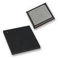
Manufacturer Part Number
PIC18F65K90T-I/MR
Description
32kB Flash, 2kB RAM, 1kB EE, NanoWatt XLP, LCD 64 QFN 9x9x0.9mm T/R
Manufacturer
Microchip Technology
Series
PIC® XLP™ 18Fr
Datasheet
1.PIC18F66K90-IMR.pdf
(570 pages)
Specifications of PIC18F65K90T-I/MR
Processor Series
PIC18F
Core
PIC
Data Bus Width
8 bit
Program Memory Type
Flash
Program Memory Size
32 KB
Data Ram Size
2 KB
Interface Type
I2C, SPI
Maximum Clock Frequency
64 MHz
Number Of Timers
8
Operating Supply Voltage
1.8 V to 5.5 V
Maximum Operating Temperature
+ 125 C
3rd Party Development Tools
52715-96, 52716-328, 52717-734, 52712-325, EWPIC18
Minimum Operating Temperature
- 40 C
On-chip Adc
12 bit, 16 Channel
Core Processor
PIC
Core Size
8-Bit
Speed
64MHz
Connectivity
I²C, LIN, SPI, UART/USART
Peripherals
Brown-out Detect/Reset, LCD, POR, PWM, WDT
Number Of I /o
53
Eeprom Size
1K x 8
Ram Size
2K x 8
Voltage - Supply (vcc/vdd)
1.8 V ~ 5.5 V
Data Converters
A/D 16x12b
Oscillator Type
Internal
Operating Temperature
-40°C ~ 85°C
Package / Case
64-VFQFN Exposed Pad
Lead Free Status / Rohs Status
Details


PIC18F87K90 FAMILY
COMF
Syntax:
Operands:
Operation:
Status Affected:
Encoding:
Description:
Words:
Cycles:
Example:
DS39957D-page 468
Q Cycle Activity:
Before Instruction
After Instruction
Decode
REG
REG
W
Q1
=
=
=
register ‘f’
Complement f
COMF
0 f 255
d [ 0,1 ]
a [ 0,1 ]
f dest
N, Z
The contents of register ‘f’ are
complemented. If ‘d’ is ‘ 0 ’, the result is
stored in W. If ‘d’ is ‘ 1 ’, the result is
stored back in register ‘f’.
If ‘a’ is ‘ 0 ’, the Access Bank is selected.
If ‘a’ is ‘ 1 ’, the BSR is used to select the
GPR bank.
If ‘a’ is ‘ 0 ’ and the extended instruction
set is enabled, this instruction operates
in Indexed Literal Offset Addressing
mode whenever f 95 (5Fh). See
Section 29.2.3 “Byte-Oriented and
Bit-Oriented Instructions in Indexed
Literal Offset Mode”
1
1
COMF
Read
0001
Q2
13h
13h
ECh
f {,d {,a}}
11da
REG, 0, 0
Process
Data
Q3
ffff
for details.
destination
Write to
Q4
ffff
CPFSEQ
Syntax:
Operands:
Operation:
Status Affected:
Encoding:
Description:
Words:
Cycles:
Example:
Q Cycle Activity:
If skip:
If skip and followed by 2-word instruction:
Before Instruction
After Instruction
operation
operation
operation
Decode
PC Address
W
REG
If REG
If REG
No
No
No
Q1
Q1
Q1
PC
PC
register ‘f’
2009-2011 Microchip Technology Inc.
operation
operation
operation
Compare f with W, Skip if f = W
CPFSEQ
0 f 255
a [ 0,1 ]
(f) – (W),
skip if (f) = (W)
(unsigned comparison)
None
Compares the contents of data memory
location ‘f’ to the contents of W by
performing an unsigned subtraction.
If ‘f’ = W , then the fetched instruction is
discarded and a NOP is executed
instead, making this a two-cycle
instruction.
If ‘a’ is ‘ 0 ’, the Access Bank is selected.
If ‘a’ is ‘ 1 ’, the BSR is used to select the
GPR bank.
If ‘a’ is ‘ 0 ’ and the extended instruction
set is enabled, this instruction operates
in Indexed Literal Offset Addressing
mode whenever f 95 (5Fh). See
Section 29.2.3 “Byte-Oriented and
Bit-Oriented Instructions in Indexed
Literal Offset Mode”
1
1(2)
Note: 3 cycles if skip and followed
HERE
NEQUAL
EQUAL
Read
0110
No
No
No
Q2
Q2
Q2
=
=
=
=
=
=
by a 2-word instruction.
HERE
?
?
W;
Address (EQUAL)
W;
Address (NEQUAL)
f {,a}
CPFSEQ REG, 0
:
:
001a
operation
operation
operation
Process
Data
No
No
No
Q3
Q3
Q3
ffff
for details.
operation
operation
operation
operation
No
No
No
No
Q4
Q4
Q4
ffff
Related parts for PIC18F65K90T-I/MR
Image
Part Number
Description
Manufacturer
Datasheet
Request
R

Part Number:
Description:
Manufacturer:
Microchip Technology Inc.
Datasheet:
Part Number:
Description:
Manufacturer:
Microchip Technology Inc.
Datasheet:
Part Number:
Description:
Manufacturer:
Microchip Technology Inc.
Datasheet:
Part Number:
Description:
Manufacturer:
Microchip Technology Inc.
Datasheet:
Part Number:
Description:
Manufacturer:
Microchip Technology Inc.
Datasheet:
Part Number:
Description:
Manufacturer:
Microchip Technology Inc.
Datasheet:
Part Number:
Description:
Manufacturer:
Microchip Technology Inc.
Datasheet:
Part Number:
Description:
Manufacturer:
Microchip Technology Inc.
Datasheet: