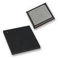
PIC18F65K90T-I/MR Microchip Technology, PIC18F65K90T-I/MR Datasheet - Page 408

PIC18F65K90T-I/MR
Manufacturer Part Number
PIC18F65K90T-I/MR
Description
32kB Flash, 2kB RAM, 1kB EE, NanoWatt XLP, LCD 64 QFN 9x9x0.9mm T/R
Manufacturer
Microchip Technology
Series
PIC® XLP™ 18Fr
Datasheet
1.PIC18F66K90-IMR.pdf
(570 pages)
Specifications of PIC18F65K90T-I/MR
Processor Series
PIC18F
Core
PIC
Data Bus Width
8 bit
Program Memory Type
Flash
Program Memory Size
32 KB
Data Ram Size
2 KB
Interface Type
I2C, SPI
Maximum Clock Frequency
64 MHz
Number Of Timers
8
Operating Supply Voltage
1.8 V to 5.5 V
Maximum Operating Temperature
+ 125 C
3rd Party Development Tools
52715-96, 52716-328, 52717-734, 52712-325, EWPIC18
Minimum Operating Temperature
- 40 C
On-chip Adc
12 bit, 16 Channel
Core Processor
PIC
Core Size
8-Bit
Speed
64MHz
Connectivity
I²C, LIN, SPI, UART/USART
Peripherals
Brown-out Detect/Reset, LCD, POR, PWM, WDT
Number Of I /o
53
Eeprom Size
1K x 8
Ram Size
2K x 8
Voltage - Supply (vcc/vdd)
1.8 V ~ 5.5 V
Data Converters
A/D 16x12b
Oscillator Type
Internal
Operating Temperature
-40°C ~ 85°C
Package / Case
64-VFQFN Exposed Pad
Lead Free Status / Rohs Status
Details
- Current page: 408 of 570
- Download datasheet (5Mb)
PIC18F87K90 FAMILY
27.1
The control registers for the CTMU are:
• CTMUCONH
• CTMUCONL
• CTMUICON
REGISTER 27-1:
DS39957D-page 408
bit 7
Legend:
R = Readable bit
-n = Value at POR
bit 7
bit 6
bit 5
bit 4
bit 3
bit 2
bit 1
bit 0
CTMUEN
R/W-0
CTMU Registers
CTMUEN: CTMU Enable bit
1 = Module is enabled
0 = Module is disabled
Unimplemented: Read as ‘ 0 ’
CTMUSIDL: Stop in Idle Mode bit
1 = Discontinue module operation when device enters Idle mode
0 = Continue module operation in Idle mode
TGEN: Time Generation Enable bit
1 = Enables edge delay generation
0 = Disables edge delay generation
EDGEN: Edge Enable bit
1 = Edges are not blocked
0 = Edges are blocked
EDGSEQEN: Edge Sequence Enable bit
1 = Edge 1 event must occur before Edge 2 event can occur
0 = No edge sequence is needed
IDISSEN: Analog Current Source Control bit
1 = Analog current source output is grounded
0 = Analog current source output is not grounded
CTTRIG: Trigger Control bit
1 = Trigger output is enabled
0 = Trigger output is disabled
U-0
—
CTMUCONH: CTMU CONTROL HIGH REGISTER
W = Writable bit
‘1’ = Bit is set
CTMUSIDL
R/W-0
R/W-0
TGEN
U = Unimplemented bit, read as ‘0’
‘0’ = Bit is cleared
EDGEN
R/W-0
The
(Register 27-1
for configuring the CTMU module edge source selec-
tion, edge source polarity selection, edge sequencing,
A/D trigger, analog circuit capacitor discharge and
enables. The CTMUICON register
bits for selecting the current source range and current
source trim.
CTMUCONH
EDGSEQEN
R/W-0
and
2009-2011 Microchip Technology Inc.
Register
and
x = Bit is unknown
IDISSEN
27-2) contain control bits
R/W-0
CTMUCONL
(Register
CTTRIG
R/W-0
27-3) has
registers
bit 0
Related parts for PIC18F65K90T-I/MR
Image
Part Number
Description
Manufacturer
Datasheet
Request
R

Part Number:
Description:
Manufacturer:
Microchip Technology Inc.
Datasheet:

Part Number:
Description:
Manufacturer:
Microchip Technology Inc.
Datasheet:

Part Number:
Description:
Manufacturer:
Microchip Technology Inc.
Datasheet:

Part Number:
Description:
Manufacturer:
Microchip Technology Inc.
Datasheet:

Part Number:
Description:
Manufacturer:
Microchip Technology Inc.
Datasheet:

Part Number:
Description:
Manufacturer:
Microchip Technology Inc.
Datasheet:

Part Number:
Description:
Manufacturer:
Microchip Technology Inc.
Datasheet:

Part Number:
Description:
Manufacturer:
Microchip Technology Inc.
Datasheet:


