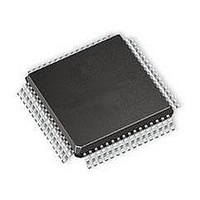
PIC18F65K90T-I/PT Microchip Technology, PIC18F65K90T-I/PT Datasheet - Page 373

PIC18F65K90T-I/PT
Manufacturer Part Number
PIC18F65K90T-I/PT
Description
32kB Flash, 2kB RAM, 1kB EE, NanoWatt XLP, LCD 64 TQFP 10x10x1mm T/R
Manufacturer
Microchip Technology
Series
PIC® XLP™ 18Fr
Datasheet
1.PIC18F66K90-IMR.pdf
(570 pages)
Specifications of PIC18F65K90T-I/PT
Processor Series
PIC18F
Core
PIC
Data Bus Width
8 bit
Program Memory Type
Flash
Program Memory Size
32 KB
Data Ram Size
2 KB
Interface Type
I2C, SPI
Maximum Clock Frequency
64 MHz
Number Of Timers
8
Operating Supply Voltage
1.8 V to 5.5 V
Maximum Operating Temperature
+ 125 C
3rd Party Development Tools
52715-96, 52716-328, 52717-734, 52712-325, EWPIC18
Minimum Operating Temperature
- 40 C
On-chip Adc
12 bit, 16 Channel
Core Processor
PIC
Core Size
8-Bit
Speed
64MHz
Connectivity
I²C, LIN, SPI, UART/USART
Peripherals
Brown-out Detect/Reset, LCD, POR, PWM, WDT
Number Of I /o
53
Eeprom Size
1K x 8
Ram Size
2K x 8
Voltage - Supply (vcc/vdd)
1.8 V ~ 5.5 V
Data Converters
A/D 16x12b
Oscillator Type
Internal
Operating Temperature
-40°C ~ 85°C
Package / Case
64-TQFP
Lead Free Status / Rohs Status
Details
Available stocks
Company
Part Number
Manufacturer
Quantity
Price
Company:
Part Number:
PIC18F65K90T-I/PT
Manufacturer:
Microchip Technology
Quantity:
10 000
Company:
Part Number:
PIC18F65K90T-I/PTRSL
Manufacturer:
Microchip Technology
Quantity:
10 000
- Current page: 373 of 570
- Download datasheet (5Mb)
23.0
The Analog-to-Digital (A/D) Converter module in the
PIC18F87K90 family of devices has 16 inputs for the
64-pin devices and 24 inputs for the 80-pin devices.
This module allows conversion of an analog input
signal to a corresponding signed 12-bit digital number.
The module has these registers:
• A/D Control Register 0 (ADCON0)
• A/D Control Register 1 (ADCON1)
• A/D Control Register 2 (ADCON2)
• A/D Port Configuration Register 0 (ANCON0)
• A/D Port Configuration Register 1 (ANCON1)
• A/D Port Configuration Register 2 (ANCON2)
• ADRESH (the upper A/D Results register)
• ADRESL (the lower A/D Results register)
The ADCON0 register, shown in
trols the operation of the A/D module. The ADCON1
register, shown in
reference and special trigger selection. The ADCON2
register, shown in
clock source and programmed acquisition time and
justification.
2009-2011 Microchip Technology Inc.
12-BIT ANALOG-TO-DIGITAL
CONVERTER (A/D) MODULE
Register
Register
23-2, configures the voltage
23-3, configures the A/D
Register
23-1, con-
PIC18F87K90 FAMILY
23.1
The converter in PIC18F87K90 family devices is
implemented as a differential A/D where the differential
voltage between two channels is measured and
converted to digital values (see
The converter can also be configured to measure a
voltage from a single input by clearing the CHSN bits
(ADCON1<2:0>). With this configuration, the negative
channel input is connected internally to AV
Figure
FIGURE 23-1:
Differential conversion feeds the two input channels to
a unity gain differential amplifier. The positive channel
input is selected using the CHS bits (ADCON0<6:2>)
and the negative channel input is selected using the
CHSN bits (ADCON1<2:0>).
The output from the amplifier is fed to the A/D convert,
as shown in
on the ADRESH and ADRESL registers. There is also
a sign bit, along with the 12-bit result, indicating if the
result is a positive or negative value.
FIGURE 23-2:
In the Single Channel Measurement mode, the
negative input is connected to A
CHSN bits (ADCON1<2:0>).
Positive input
CHS<4:0>
CHSN<2:0>
= 000
Positive input
CHS<4:0>
Negative input
CHSN<2:0>
23-2).
Differential A/D Converter
AV
Figure
SS
+
23-1. The 12-bit result is available
–
+
–
DIFFERENTIAL CHANNEL
MEASUREMENT
SINGLE CHANNEL
MEASUREMENT
Figure
VSS
DS39957D-page 373
23-1).
by clearing the
ADC
ADC
SS
(see
Related parts for PIC18F65K90T-I/PT
Image
Part Number
Description
Manufacturer
Datasheet
Request
R

Part Number:
Description:
Manufacturer:
Microchip Technology Inc.
Datasheet:

Part Number:
Description:
Manufacturer:
Microchip Technology Inc.
Datasheet:

Part Number:
Description:
Manufacturer:
Microchip Technology Inc.
Datasheet:

Part Number:
Description:
Manufacturer:
Microchip Technology Inc.
Datasheet:

Part Number:
Description:
Manufacturer:
Microchip Technology Inc.
Datasheet:

Part Number:
Description:
Manufacturer:
Microchip Technology Inc.
Datasheet:

Part Number:
Description:
Manufacturer:
Microchip Technology Inc.
Datasheet:

Part Number:
Description:
Manufacturer:
Microchip Technology Inc.
Datasheet:


