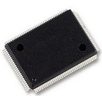
MT48LC2M32B2P-6:G Micron Technology Inc, MT48LC2M32B2P-6:G Datasheet - Page 29

MT48LC2M32B2P-6:G
Manufacturer Part Number
MT48LC2M32B2P-6:G
Description
IC, SDRAM, 64MBIT, 166MHZ, TSOP-86
Manufacturer
Micron Technology Inc
Type
SDRAMr
Series
-r
Specifications of MT48LC2M32B2P-6:G
Organization
2Mx32
Density
64Mb
Address Bus
13b
Access Time (max)
17/7.5/5.5ns
Maximum Clock Rate
166MHz
Operating Supply Voltage (typ)
3.3V
Package Type
TSOP-II
Operating Temp Range
0C to 70C
Operating Supply Voltage (max)
3.6V
Operating Supply Voltage (min)
3V
Supply Current
180mA
Pin Count
86
Mounting
Surface Mount
Operating Temperature Classification
Commercial
Memory Type
DRAM - Sychronous
Access Time
5.5ns
Page Size
64Mbit
Memory Case Style
TSOP
No. Of Pins
86
Operating Temperature Range
0°C To +70°C
Frequency
166MHz
Supply Voltage
3.3V
Format - Memory
RAM
Memory Size
64M (2Mx32)
Speed
167MHz
Interface
Parallel
Voltage - Supply
3 V ~ 3.6 V
Operating Temperature
0°C ~ 70°C
Package / Case
86-TFSOP (0.400", 10.16mm Width)
Filter Terminals
SMD
Rohs Compliant
Yes
Lead Free Status / RoHS Status
Compliant
Lead Free Status / RoHS Status
Compliant, Lead free / RoHS Compliant
Available stocks
Company
Part Number
Manufacturer
Quantity
Price
Part Number:
MT48LC2M32B2P-6:G
Manufacturer:
MICRON
Quantity:
20 000
Figure 20:
PDF: 09005aef80725c0b/Source: 09005aef806fc13c
64MSDRAM_2.fm - Rev. M 10/07 EN
WRITE-to-WRITE
Note:
COMMAND
Data for any WRITE burst may be truncated with a subsequent READ command, and
data for a fixed-length WRITE burst may be immediately followed by a subsequent
READ command. After the READ command is registered, the data inputs will be ignored,
and writes will not be executed. An example is shown in Figure 22 on page 30. Data n + 1
is either the last of a burst of two or the last desired of a longer burst.
Data for a fixed-length WRITE burst may be followed by, or truncated with, a
PRECHARGE command to the same bank (provided that auto precharge was not acti-
vated), and a full-page WRITE burst may be truncated with a PRECHARGE command to
the same bank. The PRECHARGE command should be issued
which the last desired input data element is registered. The auto precharge mode
requires a
truncating a WRITE burst, the DQM signal must be used to mask input data for the clock
edge prior to, and the clock edge coincident with, the PRECHARGE command. An
example is shown in Figure 23 on page 31. Data n + 1 is either the last of a burst of two or
the last desired of a longer burst. Following the PRECHARGE command, a subsequent
command to the same bank cannot be issued until
In the case of a fixed-length burst being executed to completion, a PRECHARGE
command issued at the optimum time (as described above) provides the same opera-
tion that would result from the same fixed-length burst with auto precharge. The disad-
vantage of the PRECHARGE command is that it requires that the command and address
buses be available at the appropriate time to issue the command; the advantage of the
PRECHARGE command is that it can be used to truncate fixed-length or full-page
bursts.
ADDRESS
DQM is LOW. Each WRITE command may be to any bank.
TRANSITIONING DATA
CLK
DQ
t
WR of at least one clock plus time, regardless of frequency. In addition, when
WRITE
BANK,
COL n
D
T0
n
IN
n + 1
NOP
T1
D
IN
DON’T CARE
WRITE
BANK,
COL b
T2
D
b
IN
29
Micron Technology, Inc., reserves the right to change products or specifications without notice.
t
RP is met.
64Mb: x4, x8, x16 SDRAM
t
WR after the clock edge at
©2000 Micron Technology, Inc. All rights reserved.
Commands


