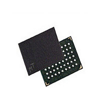
MT45W1MW16BDGB-708 IT TR Micron Technology Inc, MT45W1MW16BDGB-708 IT TR Datasheet - Page 36

MT45W1MW16BDGB-708 IT TR
Manufacturer Part Number
MT45W1MW16BDGB-708 IT TR
Description
Manufacturer
Micron Technology Inc
Datasheet
1.MT45W1MW16BDGB-708_IT_TR.pdf
(59 pages)
Specifications of MT45W1MW16BDGB-708 IT TR
Operating Temperature (max)
85C
Operating Temperature (min)
-40C
Mounting
Surface Mount
Operating Temperature Classification
Industrial
Lead Free Status / RoHS Status
Compliant
Table 15:
Figure 26:
Table 16:
PDF: 09005aef81cb58ed/Source: 09005aef81c7a667
16mb_burst_cr1_0_p23z_2.fm - Rev. H 4/08 EN
Parameter
Parameter
CE# HIGH between subsequent burst and
mixed-mode operations
Maximum CE# pulse width
CE# LOW to WAIT valid
Clock period
CE# setup to CLK active edge
Hold time from active CLK edge
Chip disable to WAIT High-Z output
CLK rise or fall time
Clock to WAIT valid
CLK HIGH or LOW time
Setup time to active CLK edge
Initialization period (required before normal operations)
Burst WRITE Cycle Timing Requirements
Initialization Timing Parameters
Initialization Period
Notes:
1. When configured for synchronous mode (BCR[15] = 0), a refresh opportunity must be pro-
Vcc, VccQ = 1.7V
vided every
tions: a) clocked CE# HIGH, or b) CE# HIGH for greater than 15ns.
16Mb: 1 Meg x 16 Async/Page/Burst CellularRAM 1.0 Memory
t
CEM. A refresh opportunity is satisfied by either of the following two condi-
Symbol
t
t
t
t
t
CBPH
KHKL
KHTL
t
t
CEM
CEW
t
t
t
CLK
CSP
t
HD
HZ
KP
SP
36
Min
t
9.62
PU
5
1
3
2
3
3
104 MHz
Micron Technology, Inc., reserves the right to change products or specifications without notice.
Max
7.5
1.6
20
20
8
8
7
Symbol
t
PU
normal operation
Device ready for
Min
12.5
4.5
5
1
2
4
3
80 MHz
Vcc (MIN)
Min
Timing Requirements
Max
7.5
1.8
©2005 Micron Technology, Inc. All rights reserved.
20
20
8
8
9
-70
Max
150
Units
ns
µs
ns
ns
ns
ns
ns
ns
ns
ns
ns
Units
Notes
µs
1
1


