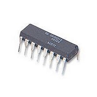
PCF8591P NXP Semiconductors, PCF8591P Datasheet - Page 5

PCF8591P
Manufacturer Part Number
PCF8591P
Description
IC, A/D AND D/A CONVERTER, 8BIT, 16-DIP
Manufacturer
NXP Semiconductors
Type
General Purposer
Specifications of PCF8591P
Number Of Channels
1
Number Of Adc's
1
Number Of Dac's
1
Adc/dac Resolution
8b
Interface Type
Serial (I2C)
Operating Supply Voltage (typ)
3.3/5V
Sample Rate
11.1KSPS
Number Of Adc Inputs
4
Number Of Dac Outputs
1
Operating Supply Voltage (max)
6V
Operating Supply Voltage (min)
2.5V
Operating Temperature (max)
85C
Operating Temperature (min)
-40C
Pin Count
16
Mounting
Through Hole
Supply Voltage Range
2.5V To 6V
Operating Temperature Range
-40°C To +85°C
Digital Ic Case Style
DIP
No. Of Pins
16
Linearity Error -
1.5LSB
Termination Type
DIP
Supply Voltage Max
8V
Input Channels Per Adc
1
Rohs Compliant
Yes
Filter Terminals
DIP
Conversion Time
90µs
Data Interface
I2C, Serial
Lead Free Status / RoHS Status
Compliant
Available stocks
Company
Part Number
Manufacturer
Quantity
Price
Company:
Part Number:
PCF8591P
Manufacturer:
SANYO
Quantity:
20 200
Company:
Part Number:
PCF8591P
Manufacturer:
NXP
Quantity:
5 510
Philips Semiconductors
7
7.1
Each PCF8591 device in an I
sending a valid address to the device. The address
consists of a fixed part and a programmable part. The
programmable part must be set according to the address
pins A0, A1 and A2. The address always has to be sent as
the first byte after the start condition in the I
protocol. The last bit of the address byte is the
read/write-bit which sets the direction of the following data
transfer (see Figs 4, 16 and 17).
2003 Jan 27
handbook, halfpage
8-bit A/D and D/A converter
FUNCTIONAL DESCRIPTION
Addressing
Fig.3 Pinning diagram (SO16).
AIN0
AIN1
AIN2
AIN3
V SS
A0
A1
A2
1
2
3
4
5
6
7
8
PCF8591T
2
C-bus system is activated by
MBL823
16
15
14
13
12
11
10
9
V DD
AOUT
V REF
AGND
EXT
OSC
SCL
SDA
2
C-bus
5
7.2
The second byte sent to a PCF8591 device will be stored
in its control register and is required to control the device
function. The upper nibble of the control register is used for
enabling the analog output, and for programming the
analog inputs as single-ended or differential inputs. The
lower nibble selects one of the analog input channels
defined by the upper nibble (see Fig.5). If the
auto-increment flag is set, the channel number is
incremented automatically after each A/D conversion.
If the auto-increment mode is desired in applications
where the internal oscillator is used, the analog output
enable flag in the control byte (bit 6) should be set. This
allows the internal oscillator to run continuously, thereby
preventing conversion errors resulting from oscillator
start-up delay. The analog output enable flag may be reset
at other times to reduce quiescent power consumption.
The selection of a non-existing input channel results in the
highest available channel number being allocated.
Therefore, if the auto-increment flag is set, the next
selected channel will be always channel 0. The most
significant bits of both nibbles are reserved for future
functions and have to be set to logic 0. After a Power-on
reset condition all bits of the control register are reset to
logic 0. The D/A converter and the oscillator are disabled
for power saving. The analog output is switched to a
high-impedance state.
handbook, halfpage
Control byte
msb
1
fixed part
0
Fig.4 Address byte.
0
1
programmable part
A2
A1
Product specification
A0
PCF8591
MBL824
R/W
lsb


