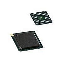
LPC1850FET256,551 NXP Semiconductors, LPC1850FET256,551 Datasheet - Page 50

LPC1850FET256,551
Manufacturer Part Number
LPC1850FET256,551
Description
MCU 32BIT ARM CORTEX M3 256BGA
Manufacturer
NXP Semiconductors
Series
LPC18xxr
Datasheet
1.LPC1830FET256551.pdf
(87 pages)
Specifications of LPC1850FET256,551
Core Processor
ARM® Cortex-M3™
Core Size
32-Bit
Speed
150MHz
Connectivity
CAN, EBI/EMI, Ethernet, I²C, IrDA, Microwire, QEI, SD/MMC, SPI, SSI, SSP, UART/USART, USB, USB OTG
Peripherals
Brown-out Detect/Reset, DMA, I²S, LCD, POR, PWM, WDT
Number Of I /o
80
Program Memory Size
-
Program Memory Type
ROMless
Eeprom Size
-
Ram Size
200K x 8
Voltage - Supply (vcc/vdd)
2.2 V ~ 3.6 V
Data Converters
A/D 8x10b; D/A 1x10b
Oscillator Type
Internal
Operating Temperature
-40°C ~ 85°C
Package / Case
256-LBGA
Processor Series
LPC1850
Core
ARM Cortex M3
Data Bus Width
32 bit
Data Ram Size
200 KB
Interface Type
SPI Flash (SPIFI), USB, Ethernet, LCD, External Memory Controller, I2C
Maximum Clock Frequency
150 MHz
Number Of Programmable I/os
80
Number Of Timers
6
Operating Supply Voltage
2 V to 3.6 V
Maximum Operating Temperature
+ 85 C
Mounting Style
SMD/SMT
Minimum Operating Temperature
- 40 C
Operating Temperature Range
- 40 C to + 85 C
Lead Free Status / Rohs Status
Lead free / RoHS Compliant
Other names
568-6682
Available stocks
Company
Part Number
Manufacturer
Quantity
Price
Company:
Part Number:
LPC1850FET256,551
Manufacturer:
NXP Semiconductors
Quantity:
10 000
Part Number:
LPC1850FET256,551
Manufacturer:
NXP/恩智浦
Quantity:
20 000
NXP Semiconductors
LPC1850_30_20_10
Objective data sheet
7.17.2 System Control Unit (SCU)
7.17.3 Clock Generation Unit (CGU)
7.17.4 Internal RC oscillator (IRC)
7.17.5 PLL0 (for USB0)
7.17.6 System PLL1
7.17.7 Reset Generation Unit (RGU)
In addition, the CREG block contains the part identification and part configuration
information.
The system control unit determines the function and electrical mode of the digital pins. By
default function 0 is selected for all pins with pull-up enabled.
Analog I/Os for the ADCs and the DAC as well as most USB pins are on separate pads
and are not controlled through the SCU.
The Clock Generator Unit (CGU) generates several base clocks. The base clocks may be
unrelated in frequency and phase and can have different clock sources within the CGU.
One CGU base clock is routed to the CLKOUT pins.
Derived from each base clock may be multiple branch clocks. The branch clocks offer
very flexible control for power-management purposes. All branch clocks are outputs of
one of two Clock Control Units (CCUs) and can be controlled independently. Branch
clocks derived from the same base clock are synchronous in frequency and phase.
The IRC is used as the clock source for the WWDT and/or as the clock that drives the
PLLs and subsequently the CPU. The nominal IRC frequency is 12 MHz. The IRC is
trimmed to 1 % accuracy over the entire voltage and temperature range.
Upon power-up or any chip reset, the LPC1850/30/20/10 use the IRC as the clock source.
Software may later switch to one of the other available clock sources.
PLL0 is a dedicated PLL for the USB0 High-speed controller.
PLL0 accepts an input clock frequency from an external oscillator in the range of 14 kHz
to 25 MHz. The input frequency is multiplied up to a high frequency with a Current
Controlled Oscillator (CCO). The CCO operates in the range of 4.3 MHz to 550 MHz.
The PLL1 accepts an input clock frequency from an external oscillator in the range of
10 MHz to 25 MHz. The input frequency is multiplied up to a high frequency with a Current
Controlled Oscillator (CCO). The multiplier can be an integer value from 1 to 32. The CCO
operates in the range of 156 MHz to 320 MHz, so there is an additional divider in the loop
to keep the CCO within its frequency range while the PLL is providing the desired output
frequency. The output divider may be set to divide by 2, 4, 8, or 16 to produce the output
clock. Since the minimum output divider value is 2, it is insured that the PLL output has a
50 % duty cycle. The PLL is turned off and bypassed following a chip reset and may be
enabled by software. The program must configure and activate the PLL, wait for the PLL
to lock, and then connect to the PLL as a clock source. The PLL settling time is 100 s.
The RGU allows generation of independent reset signals for individual blocks and
peripherals.
All information provided in this document is subject to legal disclaimers.
Rev. 1.2 — 17 February 2011
32-bit ARM Cortex-M3 microcontroller
LPC1850/30/20/10
© NXP B.V. 2011. All rights reserved.
50 of 87


