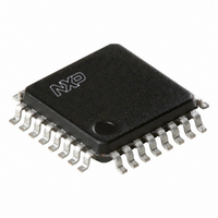
PCK940LBD,151 NXP Semiconductors, PCK940LBD,151 Datasheet

PCK940LBD,151
Specifications of PCK940LBD,151
935281611151
PCK940LBD-S
Available stocks
Related parts for PCK940LBD,151
PCK940LBD,151 Summary of contents
Page 1
PCK940L Low voltage clock distribution chip Rev. 01 — 4 April 2006 1. General description The PCK940L low voltage clock distribution chip with 2 3.3 V LVCMOS output capabilities. The ...
Page 2
Philips Semiconductors I Dual or single supply voltage: N Dual V N Single 3 Single 2 Ordering information Table 1. Type number PCK940LBD 4. Functional diagram Fig 1. Functional diagram of PCK940L PCK940L_1 Product ...
Page 3
Philips Semiconductors 5. Pinning information 5.1 Pinning Fig 2. Pin configuration for LQFP32 5.2 Pin description Table 2. Symbol PECL_CLK PECL_CLK LVCMOS_CLK LVCMOS_CLKSEL Q0 to Q17 GND1 GND2 V CC1 V CC2 PCK940L_1 Product data sheet GND1 1 GND2 2 ...
Page 4
Philips Semiconductors 6. Functional description Refer to 6.1 Function table Table 3. LVCMOS_CLKSEL 0 1 Table 4. Supply pin V CC2 V CC1 7. Limiting values Table 5. In accordance with the Absolute Maximum Rating System (IEC 60134). Symbol V ...
Page 5
Philips Semiconductors Table 7. Static characteristics (3 3.3 V amb CC2 Symbol Parameter V HIGH-level input voltage IH V LOW-level input voltage IL V peak-to-peak input voltage i(p-p) V ...
Page 6
Philips Semiconductors 9. Dynamic characteristics Table 9. Dynamic characteristics (3 3.3 V amb CC2 Symbol Parameter f maximum operating frequency oper(max) t LOW-to-HIGH propagation PLH delay t output skew ...
Page 7
Philips Semiconductors Table 10. Dynamic characteristics (3 3.3 V amb CC2 Symbol Parameter f maximum operating frequency oper(max) t LOW-to-HIGH propagation PLH delay t output skew time sk(o) t ...
Page 8
Philips Semiconductors Table 11. Dynamic characteristics (2 2.5 V amb CC2 Symbol Parameter f maximum operating frequency oper(max) t LOW-to-HIGH propagation PLH delay t output skew time sk(o) t ...
Page 9
Philips Semiconductors 9.1 Timing diagrams PECL_CLK V i(p-p) PECL_CLK Fig 3. Propagation delay (t ) test reference 100 %) The time from the PLL controlled edge ...
Page 10
Philips Semiconductors 10. Test information Fig 8. LVCMOS_CLK PCK940L AC test reference for V Fig 9. PECL_CLK PCK940L AC test reference for V PCK940L_1 Product data sheet Low voltage clock distribution chip DIFFERENTIAL ...
Page 11
Philips Semiconductors 11. Package outline LQFP32: plastic low profile quad flat package; 32 leads; body 1 pin 1 index DIMENSIONS (mm are the original dimensions) ...
Page 12
Philips Semiconductors 12. Soldering 12.1 Introduction to soldering surface mount packages This text gives a very brief insight to a complex technology. A more in-depth account of soldering ICs can be found in our Data Handbook IC26; Integrated Circuit Packages ...
Page 13
Philips Semiconductors – smaller than 1.27 mm, the footprint longitudinal axis must be parallel to the transport direction of the printed-circuit board. The footprint must incorporate solder thieves at the downstream end. • For packages with leads on four sides, ...
Page 14
Philips Semiconductors [4] These packages are not suitable for wave soldering. On versions with the heatsink on the bottom side, the solder cannot penetrate between the printed-circuit board and the heatsink. On versions with the heatsink on the top side, ...
Page 15
Philips Semiconductors 15. Legal information 15.1 Data sheet status [1][2] Document status Product status Objective [short] data sheet Development Preliminary [short] data sheet Qualification Product [short] data sheet Production [1] Please consult the most recently issued document before initiating or ...
Page 16
Philips Semiconductors 17. Contents 1 General description . . . . . . . . . . . . . . . . . . . . . . 1 2 Features . . . . . . . . ...


