PCK9446BD,151 NXP Semiconductors, PCK9446BD,151 Datasheet - Page 9
PCK9446BD,151
Manufacturer Part Number
PCK9446BD,151
Description
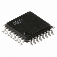
IC FANOUT BUFFER LVCMOS 32LQFP
Manufacturer
NXP Semiconductors
Type
Fanout Buffer (Distribution), Divider, Multiplexerr
Datasheet
1.PCK9446BD151.pdf
(17 pages)
Specifications of PCK9446BD,151
Number Of Circuits
1
Ratio - Input:output
2:10
Differential - Input:output
No/No
Input
LVCMOS
Output
LVCMOS
Frequency - Max
250MHz
Voltage - Supply
2.375 V ~ 3.465 V
Operating Temperature
-40°C ~ 85°C
Mounting Type
Surface Mount
Package / Case
32-LQFP
Frequency-max
250MHz
Lead Free Status / RoHS Status
Lead free / RoHS Compliant
Other names
568-3643-5
935280839151
PCK9446BD-S
935280839151
PCK9446BD-S
Available stocks
Company
Part Number
Manufacturer
Quantity
Price
Company:

Part Number:
PCK9446BD,151
Manufacturer:
NXP Semiconductors
Quantity:
10 000


Philips Semiconductors
11. Application information
PCK9446_1
Product data sheet
11.1 Driving transmission lines
The PCK9446 clock driver was designed to drive high speed signals in a terminated
transmission line environment. To provide the optimum flexibility to the user the output
drivers were designed to exhibit the lowest impedance possible. With an output
impedance of less than 20
transmission lines.
In most high performance clock networks point-to-point distribution of signals is the
method of choice. In a point-to-point scheme either series terminated or parallel
terminated transmission lines can be used. The parallel technique terminates the signal at
the end of the line with a 50
level of DC current and thus only a single terminated line can be driven by each output of
the PCK9446 clock driver. For the series terminated case however there is no DC current
draw, thus the outputs can drive multiple series terminated lines.
output driving a single series terminated line versus two series terminated lines in parallel.
When taken to its extreme, the fan-out of the PCK9446 clock driver is effectively doubled
due to its capability to drive multiple lines.
Fig 3. Single versus dual transmission lines
IN
IN
Rev. 01 — 10 April 2006
PCK9446
PCK9446
OUTPUT
BUFFER
OUTPUT
BUFFER
the drivers can drive either parallel or series terminated
resistance to 0.5V
14
14
R o
R o
R s = 36
R s = 36
R s = 36
2.5 V and 3.3 V LVCMOS clock fan-out buffer
CC
Z o = 50
Z o = 50
Z o = 50
. This technique draws a fairly high
© Koninklijke Philips Electronics N.V. 2006. All rights reserved.
002aaa708
OutA
OutB0
OutB1
Figure
PCK9446
3, illustrates an
9 of 17
Related parts for PCK9446BD,151
Image
Part Number
Description
Manufacturer
Datasheet
Request
R

Part Number:
Description:
2.5 V And 3.3 V Lvcmos Clock Fan-out Buffer
Manufacturer:
NXP Semiconductors
Datasheet:
Part Number:
Description:
NXP Semiconductors designed the LPC2420/2460 microcontroller around a 16-bit/32-bitARM7TDMI-S CPU core with real-time debug interfaces that include both JTAG andembedded trace
Manufacturer:
NXP Semiconductors
Datasheet:

Part Number:
Description:
NXP Semiconductors designed the LPC2458 microcontroller around a 16-bit/32-bitARM7TDMI-S CPU core with real-time debug interfaces that include both JTAG andembedded trace
Manufacturer:
NXP Semiconductors
Datasheet:
Part Number:
Description:
NXP Semiconductors designed the LPC2468 microcontroller around a 16-bit/32-bitARM7TDMI-S CPU core with real-time debug interfaces that include both JTAG andembedded trace
Manufacturer:
NXP Semiconductors
Datasheet:
Part Number:
Description:
NXP Semiconductors designed the LPC2470 microcontroller, powered by theARM7TDMI-S core, to be a highly integrated microcontroller for a wide range ofapplications that require advanced communications and high quality graphic displays
Manufacturer:
NXP Semiconductors
Datasheet:
Part Number:
Description:
NXP Semiconductors designed the LPC2478 microcontroller, powered by theARM7TDMI-S core, to be a highly integrated microcontroller for a wide range ofapplications that require advanced communications and high quality graphic displays
Manufacturer:
NXP Semiconductors
Datasheet:
Part Number:
Description:
The Philips Semiconductors XA (eXtended Architecture) family of 16-bit single-chip microcontrollers is powerful enough to easily handle the requirements of high performance embedded applications, yet inexpensive enough to compete in the market for hi
Manufacturer:
NXP Semiconductors
Datasheet:
Part Number:
Description:
The XA-S3 device is a member of Philips Semiconductors? XA(eXtended Architecture) family of high performance 16-bitsingle-chip microcontrollers
Manufacturer:
NXP Semiconductors
Datasheet:

Part Number:
Description:
The NXP BlueStreak LH75401/LH75411 family consists of two low-cost 16/32-bit System-on-Chip (SoC) devices
Manufacturer:
NXP Semiconductors
Datasheet:
Part Number:
Description:
The NXP LPC3130/3131 combine an 180 MHz ARM926EJ-S CPU core, high-speed USB2
Manufacturer:
NXP Semiconductors
Datasheet:
Part Number:
Description:
The NXP LPC3141 combine a 270 MHz ARM926EJ-S CPU core, High-speed USB 2
Manufacturer:
NXP Semiconductors
Part Number:
Description:
The NXP LPC3143 combine a 270 MHz ARM926EJ-S CPU core, High-speed USB 2
Manufacturer:
NXP Semiconductors

Part Number:
Description:
The NXP LPC3152 combines an 180 MHz ARM926EJ-S CPU core, High-speed USB 2
Manufacturer:
NXP Semiconductors
Part Number:
Description:
The NXP LPC3154 combines an 180 MHz ARM926EJ-S CPU core, High-speed USB 2
Manufacturer:
NXP Semiconductors