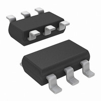
LTC6992HS6-1#TRMPBF Linear Technology, LTC6992HS6-1#TRMPBF Datasheet - Page 12

LTC6992HS6-1#TRMPBF
Manufacturer Part Number
LTC6992HS6-1#TRMPBF
Description
IC TIMERBLOX VOLT PWM TSOT23-6
Manufacturer
Linear Technology
Datasheet
1.LTC6992CDCB-1TRMPBF.pdf
(32 pages)
Specifications of LTC6992HS6-1#TRMPBF
Frequency
*
Voltage - Supply
*
Current - Supply
365µA
Operating Temperature
*
Package / Case
TSOT-23-6, TSOT-6
Count
*
Lead Free Status / RoHS Status
Lead free / RoHS Compliant
Other names
LTC6992HS6-1#TRMPBFTR
Available stocks
Company
Part Number
Manufacturer
Quantity
Price
PIN FUNCTIONS
LTC6992-1/LTC6992-2/
LTC6992-3/LTC6992-4
TYPICAL PERFORMANCE CHARACTERISTICS
otherwise noted.
V
ply should be kept free from noise and ripple. It should be
bypassed directly to the GND pin with a 0.1μF capacitor.
DIV (Pin 2/Pin 4): Programmable Divider and Polarity
Input. The DIV pin voltage (V
into a 4-bit result (DIVCODE). V
a resistor divider between V
to ensure an accurate result. The DIV pin and resistors
should be shielded from the OUT pin or any other traces
that have fast edges. Limit the capacitance on the DIV
pin to less than 100pF so that V
MSB of DIVCODE (POL) determines if the PWM signal
is inverted before driving the output. When POL = 1 the
transfer function is inverted (duty cycle decreasing as
V
SET (Pin 3/Pin 3): Frequency-Setting Input. The voltage
on the SET pin (V
amount of current sourced from the SET pin (I
grams the master oscillator frequency. The I
range is 1.25μA to 20μA. The output oscillation will stop
12
+
MOD
1V/DIV
1V/DIV
(Pin 1/Pin 5): Supply Voltage (2.25V to 5.5V). This sup-
OUT
V
+
increases).
V
DIVCODE = 3 (÷64)
R
V
Typical Start-Up, POL = 0
+
MOD
SET
= 2.5V
= 50k
= 0.3V (~25% DUTY CYCLE)
500μs
SET
100μs/DIV
) is regulated to 1V above GND. The
(DCB/S6)
+
and GND. Use 1% resistors
DIV
DIV
6992 G53
) is internally converted
DIV
may be generated by
settles quickly. The
1V/DIV
1V/DIV
OUT
V
+
SET
V
DIVCODE = 12 (÷64, POL = 1)
R
V
Typical Start-Up, POL = 1
+
MOD
SET
SET
= 2.5V
current
= 50k
= 0.2V (~87.5% DUTY CYCLE)
) pro-
500μs
100μs/DIV
if I
nected between SET and GND is the most accurate way to
set the frequency. For best performance, use a precision
metal or thin film resistor of 0.5% or better tolerance and
50ppm/°C or better temperature coefficient. For lower ac-
curacy applications an inexpensive 1% thick film resistor
may be used.
Limit the capacitance on the SET pin to less than 10pF
to minimize jitter and ensure stability. Capacitance less
than 100pF maintains the stability of the feedback circuit
regulating the V
SET
drops below approximately 500nA. A resistor con-
6992 G54
V
+
V
+
= 3.3V, R
R
SET
SET
MOD
GND
SET
0.5V/DIV
voltage.
1V/DIV
V
LTC6992
MOD
OUT
SET
125kHz Full Modulation
V
DIVCODE = 1
R
= 200k, and T
LTC6992-1
OUT
+
SET
6992 PF
DIV
= 3.3V
V
+
= 100k
C1
0.1μF
50μs/DIV
A
= 25°C, unless
V
+
R1
R2
69921234f
6992 G55


