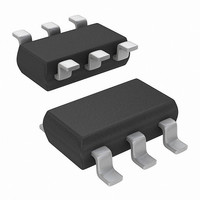
LTC6992HS6-1#TRMPBF Linear Technology, LTC6992HS6-1#TRMPBF Datasheet - Page 19

LTC6992HS6-1#TRMPBF
Manufacturer Part Number
LTC6992HS6-1#TRMPBF
Description
IC TIMERBLOX VOLT PWM TSOT23-6
Manufacturer
Linear Technology
Datasheet
1.LTC6992CDCB-1TRMPBF.pdf
(32 pages)
Specifications of LTC6992HS6-1#TRMPBF
Frequency
*
Voltage - Supply
*
Current - Supply
365µA
Operating Temperature
*
Package / Case
TSOT-23-6, TSOT-6
Count
*
Lead Free Status / RoHS Status
Lead free / RoHS Compliant
Other names
LTC6992HS6-1#TRMPBFTR
Available stocks
Company
Part Number
Manufacturer
Quantity
Price
APPLICATIONS INFORMATION
Basic Operation
The simplest and most accurate method to program the
LTC6992 is to use a single resistor, R
SET and GND pins. The design procedure is a four step
process. After choosing the proper LTC6992 version and
POL bit setting, select the N
the value for the R
Step 1: Selecting the POL Bit Setting
Most applications will use POL = 0, resulting in a positive
transfer function. However, some applications may require a
negative transfer function, where increasing V
the output duty cycle. For example, if the LTC6992 is used
in a feedback loop, POL = 1 may be required to achieve
negative feedback.
Step 2: Selecting the LTC6992 Version
The difference between the LTC6992 versions is observed at
the endpoints of the duty cycle control range. Applications
that require the output to never stop oscillating should use
the LTC6992-2. On the other hand, if the output should be
allowed to rest at GND or V
select the LTC6992-1.
The LTC6992-3 and LTC6992-4 clamp the duty cycle at
only one end of the control range, allowing the output to
stop oscillating at the other extreme. If POL = 1 the clamp
will swap from low duty cycle to high, or vice-versa. Refer
to Table 2 and Figure 4 for assistance in selecting the
proper version.
Step 3: Selecting the N
As explained earlier, the voltage on the DIV pin sets the
DIVCODE which determines both the POL bit and the
N
selected to be within the following range.
To minimize supply current, choose the lowest N
(generally recommended). For faster start-up or decreased
jitter, choose a higher N
as a guide to select the best N
plication.
DIV
62.5kHz
value. For a given output frequency, N
f
OUT
≤ N
DIV
SET
≤
1MHz
DIV
resistor.
f
OUT
DIV
setting. Alternatively, use Table 1
Frequency Divider Value
+
DIV
(0% or 100% duty cycle),
DIV
value and then calculate
value for the given ap-
SET
, between the
DIV
MOD
should be
DIV
reduces
value
(1a)
With POL already chosen, this completes the selection of
DIVCODE. Use Table 1 to select the proper resistor divider
or V
Step 4: Calculate and Select R
The final step is to calculate the correct value for R
using the following equation.
Select the standard resistor value closest to the calculated
value.
Example: Design a PWM circuit that satisfies the following
requirements:
• f
• Positive V
• Output can reach 100% duty cycle, but not 0%
• Minimum power consumption
Step 1: Selecting the POL Bit Setting
For positive transfer function (duty cycle increases with
V
Step 2: Selecting the LTC6992 Version
To limit the minimum duty cycle, but allow the maximum
duty cycle to reach 100%, choose LTC6992-4. (Note that
if POL = 1 the LTC6992-3 would be the correct choice.)
Step 3: Selecting the N
Choose an N
Equation (1a).
Potential settings for N
the best choice, as it minimizes supply current by us-
ing a large R
DIVCODE = 1. Using Table 1, choose the R1 and R2 values
to program DIVCODE = 1.
MOD
3.125 ≤ N
R
OUT
DIV
SET
), choose POL = 0.
/V
= 20kHz
=
+
LTC6992-1/LTC6992-2/
1MHz • 50k
ratio to apply to the DIV pin.
N
LTC6992-3/LTC6992-4
DIV
MOD
DIV
SET
DIV
• f
≤ 50
resistor. POL = 0 and N
to duty cycle response
value that meets the requirements of
OUT
DIV
DIV
include 4 and 16. N
Frequency Divider Value
SET
DIV
= 4 requires
DIV
19
69921234f
= 4 is
(1b)
SET


