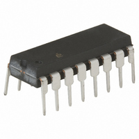
CDP68HC68T1E Intersil, CDP68HC68T1E Datasheet - Page 15

CDP68HC68T1E
Manufacturer Part Number
CDP68HC68T1E
Description
IC RTC 32X8 NVSRAM CMOS 16-DIP
Manufacturer
Intersil
Type
Clock/Calendar/NVSRAMr
Datasheet
1.CDP68HC68T1EZ.pdf
(23 pages)
Specifications of CDP68HC68T1E
Memory Size
32B
Time Format
HH:MM:SS (12/24 hr)
Date Format
YY-MM-DD-dd
Interface
SPI, 3-Wire Serial
Voltage - Supply
3 V ~ 6 V
Operating Temperature
-40°C ~ 85°C
Mounting Type
Through Hole
Package / Case
16-DIP (0.300", 7.62mm)
Lead Free Status / RoHS Status
Contains lead / RoHS non-compliant
Available stocks
Company
Part Number
Manufacturer
Quantity
Price
Company:
Part Number:
CDP68HC68T1E
Manufacturer:
INFINEON
Quantity:
36 000
Part Number:
CDP68HC68T1E
Manufacturer:
INTERSIL
Quantity:
20 000
Company:
Part Number:
CDP68HC68T1EZ
Manufacturer:
MICROCHIP
Quantity:
4 500
Company:
Part Number:
CDP68HC68T1EZ
Manufacturer:
Intersil
Quantity:
1 711
Company:
Part Number:
CDP68HC68T1EZ
Manufacturer:
TexasInstruments
Quantity:
105
Read/Write Data
Read/Write data follows the Address/Control byte.
Watchdog Reset
When watchdog operation is selected, CE must be toggled
periodically or a CPU reset will be outputted.
CPUR
NOTE: SCK can be either polarity.
SCK
CE
FIGURE 11. WATCHDOG OPERATION WAVEFORMS
SCK (NOTE)
MOSI
MISO
CE
(See Figure 10)
(See Figure 11)
SERVICE
TIME
15
D7
D7
BIT
FIGURE 10. READ/WRITE DATA TRANSFER WAVEFORMS
SERVICE
TIME
D7
7
D6
D6
D6
6
D5
D5
CDP68HC68T1
D5
5
D4
D4
D4
4
D3
D3
Address and Data
Data transfers can occur one byte at a time (Figure 12) or in
a multibyte burst mode (Figure 13). After the Real-Time
Clock enabled, an Address/Control word is sent to set the
CLOCK or RAM and select the type of operation (i.e., Read
or Write). For a single-byte Read or Write, one byte is
transferred to or from the Clock Register or RAM location
specified in the Address/Control byte and the Real-Time
Clock is then disabled. Write cycle causes the latched Clock
Register or RAM address to automatically increment.
Incrementing continues after each transfer until the device is
disabled. After incrementing to 1FH the address will “wrap”
to 00H and continue. Therefore, when the RAM is selected
the address will “wrap” to 00H and when the clock is
selected the address will “wrap” 20H.
D3
3
D2
D2
D2
2
D1
D1
D1
1
D0
D0
D0
0
October 29, 2007
FN1547.8


