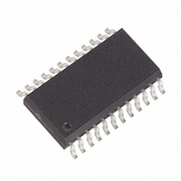
DS14285SN Maxim Integrated Products, DS14285SN Datasheet - Page 4

DS14285SN
Manufacturer Part Number
DS14285SN
Description
IC RTC W/NV RAM CNTRL IND 24SOIC
Manufacturer
Maxim Integrated Products
Type
Clock/Calendar/NVSRAMr
Datasheet
1.DS14285Q.pdf
(26 pages)
Specifications of DS14285SN
Memory Size
114B
Time Format
HH:MM:SS (12/24 hr)
Date Format
YY-MM-DD-dd
Interface
Parallel
Voltage - Supply
4.5 V ~ 5.5 V
Operating Temperature
-40°C ~ 85°C
Mounting Type
Surface Mount
Package / Case
24-SOIC (7.5mm Width)
Lead Free Status / RoHS Status
Contains lead / RoHS non-compliant
MOT (Mode Select) - The MOT pin offers the flexibility to choose between to bus types. When
connected to V
bus timing is selected. The pin has an internal pull-down resistance of approximately 20 KΩ. This pin is
on the DS14285Q only.
AS (Address Strobe Input) - A positive going address strobe pulse serves to demultiplex the bus. The
falling edge of AS/ALE causes the address to be latched within the DS14285/DS14287.
DS (Data Strobe or Read Input) - For the DS14285Q the DS/
depending on the level of the MOT pin. When the MOT pin is connected to V
selected. In this mode DS is a positive pulse during the latter portion of the bus cycle and is called Data
Strobe. During read cycles, DS signifies the time that the DS14285Q is to drive the bidirectional bus. In
write cycles the trailing edge of DS causes the DS14285Q to latch the written data. When the MOT pin is
connected to GND, Intel bus timing is selected. In this mode the DS pin is called Read(
the time period when the DS14285Q drives the bus with read data. The
as the Output Enable (
The DS14285, DS14285S and DS14287 do not have a MOT pin and therefore operate only in Intel bus
timing mode.
R/
connected to V
read or write. A read cycle is indicated with a high level on R/
indicated when R/
When the MOT pin is connected to GND for Intel timing, the R/
RAMs.
DS14285/DS14287 to be accessed.
and during
addresses but no access will occur. When V
inhibits access cycles by internally disabling the
data and RAM data during power outages.
can be used as an interrupt input to a processor. The
causing the interrupt is present and the corresponding interrupt-enable bit is set. To clear the
processor program normally reads the C register. The
When no interrupt conditions are present, the
interrupting devices can be connected to an
external pull-up resistor.
CS
WR
IRQ
W
. In this mode the R/
(Chip Select Input) - The Chip Select signal must be asserted low for a bus cycle in the
(Interrupt Request Output) - The
(Read/Write Input) - The R/
RD
CC
CC
and
, Motorola bus timing is selected. When connected to GND or left disconnected, Intel
for Motorola timing, R/
W
WR
is low during DS.
OE
) signal on a typical memory.
for Intel timing. Bus cycles which take place without asserting
W
pin has the same meaning as the Write Enable signal (
CS
W
must be kept in the active state during DS for Motorola timing
pin also has two modes of operation. When the MOT pin is
IRQ
W
IRQ
is at a level which indicates whether the current cycle is a
CC
pin is an active low output of the DS14285/DS14287 that
bus. The
is below 4.25 volts, the DS14285/DS14287 internally
CS
IRQ
4 of 26
input. This action protects both the real time clock
RESET
IRQ
level is in the high impedance state. Multiple
IRQ
output remains low as long as the status bit
pin also clears pending interrupts.
bus is an open drain output and requires an
W
W
RD
signal is an active low signal called
while DS is high. A write cycle is
pin has two modes of operation
RD
signal is the same definition
CC
, Motorola bus timing is
RD
WE
).
CS
RD
) on generic
IRQ
will latch
identifies
pin the


