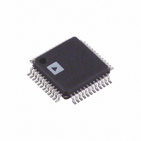
AD7663ASTZ Analog Devices Inc, AD7663ASTZ Datasheet - Page 14

AD7663ASTZ
Manufacturer Part Number
AD7663ASTZ
Description
IC ADC 16BIT CMOS 48-LQFP
Manufacturer
Analog Devices Inc
Series
PulSAR®r
Datasheet
1.AD7663ASTZ.pdf
(24 pages)
Specifications of AD7663ASTZ
Data Interface
Serial, Parallel
Number Of Bits
16
Sampling Rate (per Second)
250k
Number Of Converters
1
Power Dissipation (max)
41mW
Voltage Supply Source
Analog and Digital
Operating Temperature
-40°C ~ 85°C
Mounting Type
Surface Mount
Package / Case
48-LQFP
Resolution (bits)
16bit
Sampling Rate
250kSPS
Input Channel Type
Differential
Supply Voltage Range - Analog
4.75V To 5.25V
Lead Free Status / RoHS Status
Lead free / RoHS Compliant
For Use With
EVAL-AD7663CBZ - BOARD EVALUATION FOR AD7663
Lead Free Status / RoHS Status
Lead free / RoHS Compliant, Lead free / RoHS Compliant
Available stocks
Company
Part Number
Manufacturer
Quantity
Price
Company:
Part Number:
AD7663ASTZ
Manufacturer:
AD
Quantity:
513
Company:
Part Number:
AD7663ASTZ
Manufacturer:
Analog Devices Inc
Quantity:
10 000
Part Number:
AD7663ASTZ
Manufacturer:
ADI/亚德诺
Quantity:
20 000
Company:
Part Number:
AD7663ASTZRL
Manufacturer:
Analog Devices Inc
Quantity:
10 000
AD7663
During the acquisition phase for ac signals, the AD7663 behaves
like a one-pole RC filter consisting of the equivalent resistance of
the resistive scaler R/2 in series with R1 and C
is typically 2700 W and is a lumped component made up of some
serial resistors and the on-resistance of the switches. The capacitor
C
This one-pole filter with a typical –3 dB cutoff frequency of
800 kHz reduces undesirable aliasing effects and limits the noise
coming from the inputs.
Except when using the 0 V to 2.5 V analog input voltage range,
the AD7663 has to be driven by a very low impedance source to
avoid gain errors. That can be done by using a driver amplifier
whose choice is eased by the primarily resistive analog input
circuitry of the AD7663.
When using the 0 V to 2.5 V analog input voltage range, the input
impedance of the AD7663 is very high so the AD7663 can be
driven directly by a low impedance source without gain error.
That allows, as shown in Figure 5, putting an external one-pole
RC filter between the output of the amplifier output and the ADC
analog inputs to even further improve the noise filtering by the
AD7663 analog input circuit. However, the source impedance
has to be kept low because it affects the ac performances, especially
the total harmonic distortion (THD). The maximum source
impedance depends on the amount of THD that can be tolerated.
The THD degradation is a function of the source impedance
and the maximum input frequency as shown in Figure 8.
S
Figure 8. THD vs. Analog Input Frequency and Input
Resistance (0 V to 2.5 V Only)
is typically 60 pF and is mainly the ADC sampling capacitor.
–100
–110
75
70
65
60
55
50
45
40
35
–70
–80
–90
Figure 7. Analog Input CMRR vs. Frequency
0
10
R = 50
10
FREQUENCY – kHz
FREQUENCY – kHz
100
100
R = 11
R = 100
S
. The resistor R1
1000
1000
–14–
Driver Amplifier Choice
Although the AD7663 is easy to drive, the driver amplifier needs
to meet at least the following requirements:
The AD8021 meets these requirements and is usually appropri-
ate for almost all applications. The AD8021 needs an external
compensation capacitor of 10 pF. This capacitor should have good
linearity as an NPO ceramic or mica type.
The AD8022 could also be used where a dual version is needed
and gain of 1 is used.
The AD829 is another alternative where high frequency (above
100 kHz) performance is not required. In a gain of 1, it requires
an 82 pF compensation capacitor.
The AD8610 is also another option where low bias current is
needed in low frequency applications.
•
•
•
The driver amplifier and the AD7663 analog input circuit
have to be able, together, to settle for a full-scale step of the
capacitor array at a 16-bit level (0.0015%). In the amplifier’s
data sheet, the settling at 0.1% to 0.01% is more commonly
specified. It could significantly differ from the settling time at
16-bit level and, therefore, it should be verified prior to the
driver selection. The tiny op amp AD8021, which combines
ultralow noise and a high gain bandwidth, meets this settling
time requirement even when used with a high gain up to 13.
The noise generated by the driver amplifier needs to be kept
as low as possible in order to preserve the SNR and transition
noise performance of the AD7663. The noise coming from
the driver is first scaled down by the resistive scaler according
to the analog input voltage range used, and is then filtered by
the AD7663 analog input circuit one-pole, low-pass filter
made by (R/2 + R1) and C
the amplifier is
where:
f
N
e
FSR is the full-scale span (i.e., 5 V for ±2.5 V range).
For instance, when using the 0 V to 2.5 V range, a driver
like the AD8610 with an equivalent input noise of 6 nV/÷Hz
and configured as a buffer, thus with a noise gain of 1, the
SNR degrades by only 0.24 dB.
The driver needs to have a THD performance suitable to
that of the AD7663. TPC 10 gives the THD versus frequency
that the driver should preferably exceed.
–3 dB
N
SNR
is the –3 dB input bandwidth in MHz of the AD7663
(0.8 MHz) or the cut-off frequency of the input filter
if any used (0 V to 2.5 V range).
is the noise factor of the amplifier (1 if in buffer
configuration).
is the equivalent input noise voltage of the op amp
in nV/Hz
LOSS
=
20
1/2
log
.
Ê
Á
Á
Á
Á
Á
Ë
784
S
. The SNR degradation due to
+
p
2
f
–
3
28
dB
Ê
Á
Ë
2 5
.
FSR
N e
N
ˆ
˜
¯
2
REV. B
ˆ
˜
˜
˜
˜
˜
¯


