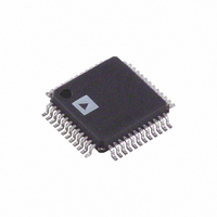
AD7663ASTZ Analog Devices Inc, AD7663ASTZ Datasheet - Page 6

AD7663ASTZ
Manufacturer Part Number
AD7663ASTZ
Description
IC ADC 16BIT CMOS 48-LQFP
Manufacturer
Analog Devices Inc
Series
PulSAR®r
Datasheet
1.AD7663ASTZ.pdf
(24 pages)
Specifications of AD7663ASTZ
Data Interface
Serial, Parallel
Number Of Bits
16
Sampling Rate (per Second)
250k
Number Of Converters
1
Power Dissipation (max)
41mW
Voltage Supply Source
Analog and Digital
Operating Temperature
-40°C ~ 85°C
Mounting Type
Surface Mount
Package / Case
48-LQFP
Resolution (bits)
16bit
Sampling Rate
250kSPS
Input Channel Type
Differential
Supply Voltage Range - Analog
4.75V To 5.25V
Lead Free Status / RoHS Status
Lead free / RoHS Compliant
For Use With
EVAL-AD7663CBZ - BOARD EVALUATION FOR AD7663
Lead Free Status / RoHS Status
Lead free / RoHS Compliant, Lead free / RoHS Compliant
Available stocks
Company
Part Number
Manufacturer
Quantity
Price
Company:
Part Number:
AD7663ASTZ
Manufacturer:
AD
Quantity:
513
Company:
Part Number:
AD7663ASTZ
Manufacturer:
Analog Devices Inc
Quantity:
10 000
Part Number:
AD7663ASTZ
Manufacturer:
ADI/亚德诺
Quantity:
20 000
Company:
Part Number:
AD7663ASTZRL
Manufacturer:
Analog Devices Inc
Quantity:
10 000
AD7663
Pin
No.
1
2
3, 6, 7,
44–48
4
5
8
9, 10
11, 12
13
14
15
16
17
18
19
20
Mnemonic
AGND
AVDD
BYTESWAP
OB/2C
SER/PAR
D[0:1]
D[2:3] or
DIVSCLK[0:1]
D[4]
or EXT/INT
D[5]
or INVSYNC
D[6]
or INVSCLK
D[7]
or RDC/SDIN
OGND
OVDD
DVDD
DGND
NC
Type Description
P
P
DI
DI
DI
DO
DI/O When SER/PAR is LOW, these outputs are used as Bit 2 and Bit 3 of the Parallel Port Data
DI/O When SER/PAR is LOW, this output is used as Bit 4 of the Parallel Port Data Output Bus.
DI/O When SER/PAR is LOW, this output is used as Bit 5 of the Parallel Port Data Output Bus.
DI/O When SER/PAR is LOW, this output is used as Bit 6 of the Parallel Port Data Output Bus.
DI/O When SER/PAR is LOW, this output is used as Bit 7 of the Parallel Port Data Output Bus.
P
P
P
P
Input Analog Power Pin. Nominally 5 V.
Bit 0 and Bit 1 of the Parallel Port Data Output Bus. When SER/PAR is HIGH, these outputs
When SER/PAR is HIGH, EXT/INT is LOW and RDC/SDIN is LOW, which is the Serial
Input/Output Interface Digital Power Ground.
Input/Output Interface Digital Power. Nominally at the same supply as the supply of the host
Digital Power. Nominally at 5 V.
Digital Power Ground.
Analog Power Ground Pin.
No Connect.
Parallel Mode Selection (8/16 Bit). When LOW, the LSB is output on D[7:0] and the MSB is output
on D[15:8]. When HIGH, the LSB is output on D[15:8] and the MSB is output on D[7:0].
Straight Binary/Binary Twos Complement. When OB/2C is HIGH, the digital output is straight
binary; when LOW, the MSB is inverted, resulting in a twos complement output from its internal
shift register.
Serial/Parallel Selection Input. When LOW, the Parallel Port is selected; when HIGH, the
Serial Interface Mode is selected and some bits of the Data bus are used as a Serial Port.
are in high impedance.
Output Bus.
Master Read after Convert Mode. These inputs, part of the Serial Port, are used to slow down,
if desired, the internal serial clock that clocks the data output. In the other serial modes, these
pins are high impedance outputs.
When SER/PAR is HIGH, this input, part of the Serial Port, is used as a digital select input for
choosing the internal or an external data clock, called respectively, Master and Slave Modes.
With EXT/INT tied LOW, the internal clock is selected on SCLK output. With EXT/INT
set to a logic HIGH, output data is synchronized to an external clock signal connected to the
SCLK input, and external clock is gated by CS.
When SER/PAR is HIGH, this input, part of the Serial Port, is used to select the active state of
the SYNC signal. When LOW, SYNC is active HIGH. When HIGH, SYNC is active LOW.
When SER/PAR is HIGH, this input, part of the Serial Port, is used to invert the SCLK signal.
It is active in both master and slave mode.
When SER/PAR is HIGH, this input, part of the Serial Port, is used as either an external data
input or a read mode selection input, depending on the state of EXT/INT.
When EXT/INT is HIGH, RDC/SDIN could be used as a data input to daisy-chain the conversion
results from two or more ADCs onto a single SDOUT line. The digital data level on SDIN is
output on DATA with a delay of 16 SCLK periods after the initiation of the read sequence.
When EXT/INT is LOW, RDC/SDIN is used to select the read mode. When RDC/SDIN is
HIGH, the previous data is output on SDOUT during conversion. When RDC/SDIN is LOW,
the data can be output on SDOUT only when the conversion is complete.
interface (5 V or 3 V).
PIN FUNCTION DESCRIPTION
–6–
REV. B


