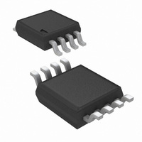
ADC121C021CIMM/NOPB National Semiconductor, ADC121C021CIMM/NOPB Datasheet - Page 27

ADC121C021CIMM/NOPB
Manufacturer Part Number
ADC121C021CIMM/NOPB
Description
IC ADC 12BIT I2C ALERT 8-MSOP
Manufacturer
National Semiconductor
Series
PowerWise®r
Datasheet
1.ADC121C021CIMMNOPB.pdf
(30 pages)
Specifications of ADC121C021CIMM/NOPB
Number Of Bits
12
Sampling Rate (per Second)
188.9k
Data Interface
I²C, Serial
Number Of Converters
1
Power Dissipation (max)
780µW
Voltage Supply Source
Single Supply
Operating Temperature
-40°C ~ 105°C
Mounting Type
Surface Mount
Package / Case
8-TSSOP, 8-MSOP (0.118", 3.00mm Width)
Number Of Elements
1
Resolution
12Bit
Architecture
SAR
Sample Rate
188.9KSPS
Input Polarity
Unipolar
Input Type
Voltage
Rated Input Volt
5.5V
Differential Input
No
Power Supply Requirement
Single
Single Supply Voltage (typ)
3.3/5V
Single Supply Voltage (min)
2.7V
Single Supply Voltage (max)
5.5V
Dual Supply Voltage (typ)
Not RequiredV
Dual Supply Voltage (min)
Not RequiredV
Dual Supply Voltage (max)
Not RequiredV
Differential Linearity Error
-0.9LSB/1LSB
Integral Nonlinearity Error
±1LSB
Operating Temp Range
-40C to 105C
Operating Temperature Classification
Industrial
Mounting
Surface Mount
Pin Count
8
Package Type
MSOP
Input Signal Type
Single-Ended
Lead Free Status / RoHS Status
Lead free / RoHS Compliant
Other names
ADC121C021CIMMTR
2.0 Applications Information
2.1 TYPICAL APPLICATION CIRCUIT
A typical application circuit is shown in
supply is bypassed with a capacitor network located close to
the ADC121C021. The ADC uses the analog supply (V
its reference voltage, so it is very important that V
clean as possible. Due to the low power requirements of the
ADC121C021, it is possible to use a precision reference as a
power supply.
The bus pull-up resistors (R
controller's supply. It is important that the pull-up resistors are
pulled to the same voltage potential as V
that the logic levels of all devices on the bus are compatible.
2.2 BUFFERED INPUT
A buffered input application circuit is shown in
analog input is buffered by a National Semiconductor
LMP7731. The non-inverting amplifier configuration provides
a buffered gain stage for a single ended source. This appli-
cation circuit is good for single-ended sensor interface. The
P
) should be powered by the
Figure
A
. This will ensure
FIGURE 18. Typical Application Circuit
18. The analog
Figure
FIGURE 19. Buffered Input Circuit
A
be kept as
19. The
A
) as
27
If the controller's supply is noisy, an appropriate bypass ca-
pacitor should be added between the controller's supply pin
and the pull-up resistors. For Hs-mode applications, this by-
pass capacitance will improve the accuracy of the ADC.
The value of the pull-up resistors (R
characteristics of each particular I
tion describes how to choose an appropriate value. As a
general rule-of-thumb, we suggest using a 1kΩ resistor for
Hs-mode bus configurations and a 5kΩ resistor for Standard
or Fast Mode bus configurations. Depending upon the bus
capacitance, these values may or may not be sufficient to
meet the timing requirements of the I
Please see the I
input must have a DC bias level that keeps the ADC input
signal from swinging below GND or above the supply (+5V in
this case).
The LM4132, with its 0.05% accuracy over temperature, is an
excellent choice as a reference source for the ADC121C021.
2
C specification for further information.
30020921
2
C bus. The I
P
30020920
2
) depends upon the
C bus specification.
2
www.national.com
C specifica-


