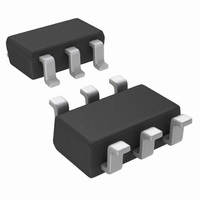
ADC121S101CIMF/NOPB National Semiconductor, ADC121S101CIMF/NOPB Datasheet - Page 13

ADC121S101CIMF/NOPB
Manufacturer Part Number
ADC121S101CIMF/NOPB
Description
IC ADC 12BIT 1MSPS SOT23-6
Manufacturer
National Semiconductor
Series
PowerWise®r
Datasheet
1.ADC121S101CIMFNOPB.pdf
(18 pages)
Specifications of ADC121S101CIMF/NOPB
Number Of Bits
12
Sampling Rate (per Second)
1M
Data Interface
DSP, MICROWIRE™, QSPI™, Serial, SPI™
Number Of Converters
1
Power Dissipation (max)
10mW
Voltage Supply Source
Single Supply
Operating Temperature
-40°C ~ 125°C
Mounting Type
Surface Mount
Package / Case
SOT-23-6
Number Of Elements
1
Resolution
12Bit
Architecture
SAR
Sample Rate
1MSPS
Input Polarity
Unipolar
Input Type
Voltage
Rated Input Volt
5.25V
Differential Input
No
Power Supply Requirement
Single
Single Supply Voltage (typ)
3.3/5V
Single Supply Voltage (min)
2.7V
Single Supply Voltage (max)
5.25V
Dual Supply Voltage (typ)
Not RequiredV
Dual Supply Voltage (min)
Not RequiredV
Dual Supply Voltage (max)
Not RequiredV
Differential Linearity Error
±1LSB
Integral Nonlinearity Error
-1.1LSB/1LSB
Operating Temp Range
-40C to 125C
Operating Temperature Classification
Automotive
Mounting
Surface Mount
Pin Count
6
Package Type
SOT-23
Input Signal Type
Single-Ended
For Use With
ADC121S101EVAL - BOARD EVALUATION FOR ADC121S101
Lead Free Status / RoHS Status
Lead free / RoHS Compliant
Other names
ADC121S101CIMF
ADC121S101CIMFTR
ADC121S101CIMFTR
Available stocks
Company
Part Number
Manufacturer
Quantity
Price
Company:
Part Number:
ADC121S101CIMF/NOPB
Manufacturer:
TI
Quantity:
3 000
SCLK frequency, the maximum guaranteed throughput is ob-
tained by using a 20 SCLK frame. As shown in
minimum allowed time between CS falling edges is deter-
mined by 1) 12.5 SCLKs for Hold mode, 2) the larger of two
quantities: either the minimum required time for Track mode
(t
or 1 SCLK padding to ensure an even number of SCLK cycles
so there is a falling SCLK edge when CS next falls.
For example, at the fastest rate for this family of parts, SCLK
is 20MHz and 2.5 SCLKs are 125ns, so the minimum time
between CS falling edges is calculated by
(12.5 SCLKs + t
maximum throughput of 1MSPS. At the slowest rate for this
family, SCLK is 1MHz. Using a 20 cycle conversion frame as
shown in
edges for a throughput of 50KSPS.
4.0 TYPICAL APPLICATION CIRCUIT
A typical application of the ADC is shown in
is provided in this example by the National Semiconductor
LP2950 low-dropout voltage regulator, available in a variety
of fixed and adjustable output voltages. The power supply pin
is bypassed with a capacitor network located close to the
ADC. Because the reference for the ADC is the supply volt-
age, any noise on the supply will degrade device noise per-
ACQ
) or 2.5 SCLKs to finish reading the result and 3) 0, 1/2
12.5*50ns + 350ns + 0.5*50ns = 1000ns
Figure 2
ACQ
yields a 20µs time between CS falling
+ 1/2 SCLK) which corresponds to a
FIGURE 5. Ideal Transfer Characteristic
Figure
Figure
6. Power
2, the
13
It is possible, however, to use fewer than 20 clock cycles pro-
vided the timing parameters are met. With a 1MHz SCLK,
there are 2500ns in 2.5 SCLK cycles, which is greater than
t
one full cycle to return to a falling edge. Thus the total time
between falling edges of CS is 12.5*1µs +2.5*1µs
+1*1µs=16µs which is a throughput of 62.5KSPS.
3.0 ADC TRANSFER FUNCTION
The output format of the ADC is straight binary. Code transi-
tions occur midway between successive integer LSB values.
The LSB width for the ADC is V
characteristic is shown in
output code of 0000 0000 0000 to a code of 0000 0000 0001
is at 1/2 LSB, or a voltage of V
occur at steps of one LSB.
formance. To keep noise off the supply, use a dedicated linear
regulator for this device, or provide sufficient decoupling from
other circuitry to keep noise off the ADC supply pin. Because
of the ADC's low power requirements, it is also possible to
use a precision reference as a power supply to maximize per-
formance. The three-wire interface is shown connected to a
microprocessor or DSP.
ACQ
. After the last data bit has come out, the clock will need
Figure
20145011
A
/8192. Other code transitions
A
5. The transition from an
/4096. The ideal transfer
www.national.com


