ADC121S101CIMF/NOPB National Semiconductor, ADC121S101CIMF/NOPB Datasheet - Page 6
ADC121S101CIMF/NOPB
Manufacturer Part Number
ADC121S101CIMF/NOPB
Description
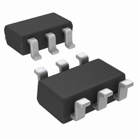
IC ADC 12BIT 1MSPS SOT23-6
Manufacturer
National Semiconductor
Series
PowerWise®r
Datasheet
1.ADC121S101CIMFNOPB.pdf
(18 pages)
Specifications of ADC121S101CIMF/NOPB
Number Of Bits
12
Sampling Rate (per Second)
1M
Data Interface
DSP, MICROWIRE™, QSPI™, Serial, SPI™
Number Of Converters
1
Power Dissipation (max)
10mW
Voltage Supply Source
Single Supply
Operating Temperature
-40°C ~ 125°C
Mounting Type
Surface Mount
Package / Case
SOT-23-6
Number Of Elements
1
Resolution
12Bit
Architecture
SAR
Sample Rate
1MSPS
Input Polarity
Unipolar
Input Type
Voltage
Rated Input Volt
5.25V
Differential Input
No
Power Supply Requirement
Single
Single Supply Voltage (typ)
3.3/5V
Single Supply Voltage (min)
2.7V
Single Supply Voltage (max)
5.25V
Dual Supply Voltage (typ)
Not RequiredV
Dual Supply Voltage (min)
Not RequiredV
Dual Supply Voltage (max)
Not RequiredV
Differential Linearity Error
±1LSB
Integral Nonlinearity Error
-1.1LSB/1LSB
Operating Temp Range
-40C to 125C
Operating Temperature Classification
Automotive
Mounting
Surface Mount
Pin Count
6
Package Type
SOT-23
Input Signal Type
Single-Ended
For Use With
ADC121S101EVAL - BOARD EVALUATION FOR ADC121S101
Lead Free Status / RoHS Status
Lead free / RoHS Compliant
Other names
ADC121S101CIMF
ADC121S101CIMFTR
ADC121S101CIMFTR
Available stocks
Company
Part Number
Manufacturer
Quantity
Price
Company:

Part Number:
ADC121S101CIMF/NOPB
Manufacturer:
TI
Quantity:
3 000


Note 7: Tested limits are guaranteed to National's AOQL (Average Outgoing Quality Level).
Note 8: This is the frequency range over which the electrical performance is guaranteed. The device is functional over a wider range which is specified under
Operating Ratings.
Note 9: Data sheet min/max specification limits are guaranteed by design, test, or statistical analysis.
Note 10: This condition is for f
= 20 MHz.
SCLK
Note 11: Minimum Quiet Time required by bus relinquish and the start of the next conversion.
Note 12: Measured with the timing test circuit shown in Figure 1 and defined as the time taken by the output signal to cross 1.0V.
Note 13: Measured with the timing test circuit shown in Figure 1 and defined as the time taken by the output signal to cross 1.0V or 2.0V.
Note 14: t
is derived from the time taken by the outputs to change by 0.5V with the timing test circuit shown in Figure 1. The measured number is then adjusted
DIS
to remove the effects of charging or discharging the output capacitance. This means that t
is the true bus relinquish time, independent of the bus loading.
DIS
www.national.com
6
Related parts for ADC121S101CIMF/NOPB
Image
Part Number
Description
Manufacturer
Datasheet
Request
R

Part Number:
Description:
National Semiconductor [8-Bit D/A Converter]
Manufacturer:
National Semiconductor
Datasheet:
Part Number:
Description:
National Semiconductor [Media Coprocessor]
Manufacturer:
National Semiconductor
Datasheet:
Part Number:
Description:
Digitally Controlled Tone and Volume Circuit with Stereo Audio Power Amplifier, Microphone Preamp Stage and National 3D Sound
Manufacturer:
National Semiconductor
Datasheet:
Part Number:
Description:
Digitally Controlled Tone and Volume Circuit with Stereo Audio Power Amplifier, Microphone Preamp Stage and National 3D Sound
Manufacturer:
National Semiconductor
Datasheet:
Part Number:
Description:
AC97 Rev 2 Codec with Sample Rate Conversion and National 3D Sound
Manufacturer:
National Semiconductor
Part Number:
Description:
Manufacturer:
National Semiconductor
Datasheet:
Part Number:
Description:
Manufacturer:
National Semiconductor
Datasheet:
Part Number:
Description:
General Purpose, Low Voltage, Low Power, Rail-to-Rail Output Operational Amplifiers
Manufacturer:
National Semiconductor
Datasheet:
Part Number:
Description:
8-bit 20 MSPS flash A/D converter.
Manufacturer:
National Semiconductor
Datasheet:
Part Number:
Description:
Low Noise Quad Operational Amplifier
Manufacturer:
National Semiconductor
Datasheet:
Part Number:
Description:
Quad Differential Line Receivers
Manufacturer:
National Semiconductor
Datasheet:
Part Number:
Description:
Quad High Speed Trapezoidal? Bus Transceiver
Manufacturer:
National Semiconductor
Datasheet:
Part Number:
Description:
Dual Line Receiver
Manufacturer:
National Semiconductor
Datasheet:
Part Number:
Description:
TTL to 10k ECL Level Translator with Latch
Manufacturer:
National Semiconductor
Datasheet: