ADC121S101CIMF/NOPB National Semiconductor, ADC121S101CIMF/NOPB Datasheet - Page 15

ADC121S101CIMF/NOPB
Manufacturer Part Number
ADC121S101CIMF/NOPB
Description
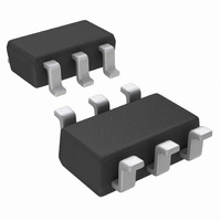
IC ADC 12BIT 1MSPS SOT23-6
Manufacturer
National Semiconductor
Series
PowerWise®r
Datasheet
1.ADC121S101CIMFNOPB.pdf
(18 pages)
Specifications of ADC121S101CIMF/NOPB
Number Of Bits
12
Sampling Rate (per Second)
1M
Data Interface
DSP, MICROWIRE™, QSPI™, Serial, SPI™
Number Of Converters
1
Power Dissipation (max)
10mW
Voltage Supply Source
Single Supply
Operating Temperature
-40°C ~ 125°C
Mounting Type
Surface Mount
Package / Case
SOT-23-6
Number Of Elements
1
Resolution
12Bit
Architecture
SAR
Sample Rate
1MSPS
Input Polarity
Unipolar
Input Type
Voltage
Rated Input Volt
5.25V
Differential Input
No
Power Supply Requirement
Single
Single Supply Voltage (typ)
3.3/5V
Single Supply Voltage (min)
2.7V
Single Supply Voltage (max)
5.25V
Dual Supply Voltage (typ)
Not RequiredV
Dual Supply Voltage (min)
Not RequiredV
Dual Supply Voltage (max)
Not RequiredV
Differential Linearity Error
±1LSB
Integral Nonlinearity Error
-1.1LSB/1LSB
Operating Temp Range
-40C to 125C
Operating Temperature Classification
Automotive
Mounting
Surface Mount
Pin Count
6
Package Type
SOT-23
Input Signal Type
Single-Ended
For Use With
ADC121S101EVAL - BOARD EVALUATION FOR ADC121S101
Lead Free Status / RoHS Status
Lead free / RoHS Compliant
Other names
ADC121S101CIMF
ADC121S101CIMFTR
ADC121S101CIMFTR
Available stocks
Company
Part Number
Manufacturer
Quantity
Price
Company:
Part Number:
ADC121S101CIMF/NOPB
Manufacturer:
TI
Quantity:
3 000
To exit shutdown mode, bring CS back low. Upon bringing
CS low, the ADC will begin powering up (power-up time is
specified in the Timing Specifications table). This power-up
delay results in the first conversion result being unusable. The
second conversion performed after power-up, however, is
valid, as shown in
If CS is brought back high before the 10th falling edge of
SCLK, the device will return to shutdown mode. This is done
to avoid accidentally entering normal mode as a result of
noise on the CS line. To exit shutdown mode and remain in
normal mode, CS must be kept low until after the 10th falling
edge of SCLK. The ADC will be fully powered-up after 16
SCLK cycles.
8.0 POWER MANAGEMENT
The ADC takes time to power-up, either after first applying
V
This corresponds to one "dummy" conversion for any SCLK
frequency within the specifications in this document. After this
first dummy conversion, the ADC will perform conversions
properly. Note that the t
tween the first dummy conversion and the second valid con-
version.
When the V
in either of the two modes: normal or shutdown. As such, one
dummy conversion should be performed after start-up, as de-
scribed in the previous paragraph. The part may then be
placed into either normal mode or the shutdown mode, as
described in Sections 7.1 and 7.2.
When the ADC is operated continuously in normal mode, the
maximum throughput is f
f
running f
fewer conversions per unit time, raising the ADC CS line after
SCLK
A
, or after returning to normal mode from shutdown mode.
. Throughput may be traded for power consumption by
SCLK
A
supply is first applied, the ADC may power up
at its maximum specified rate and performing
Figure
QUIET
SCLK
9.
time must still be included be-
/ 20 at the maximum specified
FIGURE 8. Entering Shutdown Mode
FIGURE 9. Entering Normal Mode
15
the 10th and before the 15th fall of SCLK of each conversion.
A plot of typical power consumption versus throughput is
shown in the Typical Performance Curves section. To calcu-
late the power consumption for a given throughput, multiply
the fraction of time spent in the normal mode by the normal
mode power consumption and add the fraction of time spent
in shutdown mode multiplied by the shutdown mode power
consumption. Note that the curve of power consumption vs.
throughput is essentially linear. This is because the power
consumption in the shutdown mode is so small that it can be
ignored for all practical purposes.
9.0 POWER SUPPLY NOISE CONSIDERATIONS
The charging of any output load capacitance requires current
from the power supply, V
the supply to charge the output capacitance will cause voltage
variations on the supply. If these variations are large enough,
they could degrade SNR and SINAD performance of the ADC.
Furthermore, discharging the output capacitance when the
digital output goes from a logic high to a logic low will dump
current into the die substrate, which is resistive. Load dis-
charge currents will cause "ground bounce" noise in the sub-
strate that will degrade noise performance if that current is
large enough. The larger the output capacitance, the more
current flows through the die substrate and the greater is the
noise coupled into the analog channel, degrading noise per-
formance.
To keep noise out of the power supply, keep the output load
capacitance as small as practical. It is good practice to use a
100 Ω series resistor at the ADC output, located as close to
the ADC output pin as practical. This will limit the charge and
discharge current of the output capacitance and improve
noise performance.
A
. The current pulses required from
20145016
www.national.com
20145017


