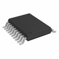
AD7822BRU Analog Devices Inc, AD7822BRU Datasheet - Page 10

AD7822BRU
Manufacturer Part Number
AD7822BRU
Description
IC ADC 8BIT 1CH 2MSPS 20TSSOP
Manufacturer
Analog Devices Inc
Datasheet
1.AD7822BRZ.pdf
(28 pages)
Specifications of AD7822BRU
Rohs Status
RoHS non-compliant
Number Of Bits
8
Sampling Rate (per Second)
2M
Data Interface
Parallel
Number Of Converters
1
Power Dissipation (max)
36mW
Voltage Supply Source
Single Supply
Operating Temperature
-40°C ~ 85°C
Mounting Type
Surface Mount
Package / Case
20-TSSOP (0.173", 4.40mm Width)
Available stocks
Company
Part Number
Manufacturer
Quantity
Price
Company:
Part Number:
AD7822BRUZ
Manufacturer:
Analog Devices Inc
Quantity:
135
Part Number:
AD7822BRUZ
Manufacturer:
ADI/亚德诺
Quantity:
20 000
AD7822/AD7825/AD7829
CIRCUIT INFORMATION
CIRCUIT DESCRIPTION
The AD7822/AD7825/AD7829 consist of a track-and-hold
amplifier followed by a half-flash analog-to-digital converter.
These devices use a half-flash conversion technique where one
4-bit flash ADC is used to achieve an 8-bit result. The 4-bit flash
ADC contains a sampling capacitor followed by 15 comparators
that compare the unknown input to a reference ladder to
achieve a 4-bit result. This first flash (that is, coarse conversion)
provides the four MSBs. For a full 8-bit reading to be realized,
a second flash (that is, fine conversion) must be performed to
provide the four LSBs. The 8-bit word is then placed on the data
output bus.
Figure 6 and Figure 7 show simplified schematics of the ADC.
When the ADC starts a conversion, the track-and-hold goes
into hold mode and holds the analog input for 120 ns. This is
the acquisition phase, as shown in Figure 6, when Switch 2 is in
Position A. At the point when the track-and-hold returns to its
track mode, this signal is sampled by the sampling capacitor,
as Switch 2 moves into Position B. The first flash occurs at this
instant and is then followed by the second flash. Typically, the
first flash is complete after 100 ns, that is, at 220 ns; and the end
of the second flash and, hence, the 8-bit conversion result is
available at 330 ns (minimum). The maximum conversion time
is 420 ns. As shown in Figure 8, the track-and-hold returns to
track mode after 120 ns and starts the next acquisition before
the end of the current conversion. Figure 10 shows the ADC
transfer function.
V
IN
T/H 1
REFERENCE
HOLD
A
TIMING AND
SW2
CONTROL
B
LOGIC
CAPACITOR
SAMPLING
Figure 6. ADC Acquisition Phase
R14
R13
R16
R15
R1
13
15
14
1
DB7
DB6
DB5
DB4
DB3
DB2
DB1
DB0
Rev. C | Page 10 of 28
V
DB0 TO DB7
TYPICAL CONNECTION DIAGRAM
Figure 9 shows a typical connection diagram for the AD7822/
AD7825/AD7829. The AGND and DGND are connected
together at the device for good noise suppression. The parallel
interface is implemented using an 8-bit data bus. The end of
conversion signal ( EOC ) idles high, the falling edge of CONVST
initiates a conversion, and at the end of conversion the falling
edge of EOC is used to initiate an interrupt service routine
(ISR) on a microprocessor (see the Parallel Interface section for
more details.) V
such as the AD780, and V
that can vary from 4.5 V to 5.5 V (see Table 5 in the Analog Input
section). When V
AD7829 power up in a low current mode, that is, power-down
mode, with the default logic level on the EOC pin on the
AD7822 and AD7825 equal to a low. Ensure the CONVST line is
not floating when V
AD7822/AD7825/AD7829 into an unknown state.
IN
CONVST
EOC
T/H 1
RD
CS
REFERENCE
HOLD
TRACK
A
TIMING AND
SW2
CONTROL
B
LOGIC
t
2
REF
120ns
CAPACITOR
HOLD
SAMPLING
DD
Figure 8. Track-and-Hold Timing
Figure 7. ADC Conversion Phase
and V
DD
is first connected, the AD7822/AD7825/
t
1
is applied, because this can put the
R14
R13
R16
R15
R1
MID
DD
are connected to a voltage source
is connected to a voltage source
13
15
14
1
TRACK
VALID
DATA
t
3
HOLD
DB7
DB6
DB5
DB4
DB3
DB2
DB1
DB0


