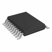
AD7822BRU Analog Devices Inc, AD7822BRU Datasheet - Page 5

AD7822BRU
Manufacturer Part Number
AD7822BRU
Description
IC ADC 8BIT 1CH 2MSPS 20TSSOP
Manufacturer
Analog Devices Inc
Datasheet
1.AD7822BRZ.pdf
(28 pages)
Specifications of AD7822BRU
Rohs Status
RoHS non-compliant
Number Of Bits
8
Sampling Rate (per Second)
2M
Data Interface
Parallel
Number Of Converters
1
Power Dissipation (max)
36mW
Voltage Supply Source
Single Supply
Operating Temperature
-40°C ~ 85°C
Mounting Type
Surface Mount
Package / Case
20-TSSOP (0.173", 4.40mm Width)
Available stocks
Company
Part Number
Manufacturer
Quantity
Price
Company:
Part Number:
AD7822BRUZ
Manufacturer:
Analog Devices Inc
Quantity:
135
Part Number:
AD7822BRUZ
Manufacturer:
ADI/亚德诺
Quantity:
20 000
TIMING CHARACTERISTICS
V
Table 2.
Parameter
t
t
t
t
t
t
t
t
t
t
t
t
t
t
t
1
2
3
4
TIMING DIAGRAM
2
1
2
3
4
5
6
7
8
9
10
11
12
13
POWER UP
POWER UP
Sample tested to ensure compliance.
See Figure 24, Figure 25, and Figure 26.
Measured with the load circuit of Figure 2 and defined as the time required for an output to cross 0.8 V or 2.4 V with V
to cross 0.4 V or 2.0 V with V
Derived from the measured time taken by the data outputs to change 0.5 V when loaded with the circuit of Figure 2. The measured number is then extrapolated back
to remove the effects of charging or discharging the 50 pF capacitor. This means that the time, t
of the part and, as such, is independent of external bus loading capacitances.
3
REF IN/OUT
4
= 2.5 V. All specifications −40°C to +85°C, unless otherwise noted.
1,
5 V ± 10%
420
20
30
110
70
10
0
0
30
10
5
20
10
15
200
25
1
DD
= 3 V ± 10%.
3 V ± 10%
420
20
30
110
70
10
0
0
30
20
5
20
10
15
200
25
1
ns max
Figure 2. Load Circuit for Access Time and Bus Relinquish Time
Unit
ns min
ns min
ns max
ns min
ns max
ns min
ns min
ns min
ns max
ns min
ns max
ns min
ns min
ns min
μs typ
μs max
TO OUTPUT
Conditions/Comments
Conversion time
Minimum CONVST pulse width
Minimum time between the rising edge of RD and the next falling edge of convert star
EOC pulse width
RD rising edge to EOC pulse high
CS to RD setup time
CS to RD hold time
Minimum RD pulse width
Data access time after RD low
Bus relinquish time after RD high
Address setup time before falling edge of RD
Address hold time after falling edge of RD
Minimum time between new channel selection and convert start
Power-up time from rising edge of CONVST using on-chip reference
Power-up time from rising edge of CONVST using external 2.5 V reference
PIN
50pF
Rev. C | Page 5 of 28
C
L
200µA
200µA
I
I
OL
OH
10
, quoted in the timing characteristics is the true bus relinquish time
2.1V
DD
AD7822/AD7825/AD7829
= 5 V ± 10%, and time required for an output


