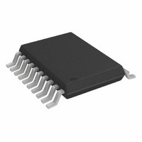
AD7822BRU Analog Devices Inc, AD7822BRU Datasheet - Page 7

AD7822BRU
Manufacturer Part Number
AD7822BRU
Description
IC ADC 8BIT 1CH 2MSPS 20TSSOP
Manufacturer
Analog Devices Inc
Datasheet
1.AD7822BRZ.pdf
(28 pages)
Specifications of AD7822BRU
Rohs Status
RoHS non-compliant
Number Of Bits
8
Sampling Rate (per Second)
2M
Data Interface
Parallel
Number Of Converters
1
Power Dissipation (max)
36mW
Voltage Supply Source
Single Supply
Operating Temperature
-40°C ~ 85°C
Mounting Type
Surface Mount
Package / Case
20-TSSOP (0.173", 4.40mm Width)
Available stocks
Company
Part Number
Manufacturer
Quantity
Price
Company:
Part Number:
AD7822BRUZ
Manufacturer:
Analog Devices Inc
Quantity:
135
Part Number:
AD7822BRUZ
Manufacturer:
ADI/亚德诺
Quantity:
20 000
PIN CONFIGURATIONS AND FUNCTION DESCRIPTIONS
Table 4. Pin Function Descriptions
Mnemonic
V
V
AGND
DGND
CONVST
EOC
CS
PD
RD
A0 to A2
DB0 to DB7
V
V
IN1
DD
REF IN/OUT
MID
to V
CONVST
DGND
IN8
EOC
DB2
DB1
DB0
RD
NC
CS
PD
Figure 3. Pin Configuration
10
1
2
3
4
5
6
7
8
9
NC = NO CONNECT
Description
Analog Input Channels. The AD7822 has a single input channel; the AD7825 and AD7829 have four and eight analog input
channels, respectively. The inputs have an input span of 2.5 V and 2 V depending on the supply voltage (V
be centered anywhere in the range AGND to V
2 V (V
Positive Supply Voltage, 3 V ± 10% and 5 V ± 10%.
Analog Ground. Ground reference for track-and-hold, comparators, reference circuit, and multiplexer.
Digital Ground. Ground reference for digital circuitry.
Logic Input Signal. The convert start signal initiates an 8-bit analog-to-digital conversion on the falling edge of this signal. The
falling edge of this signal places the track-and-hold in hold mode. The track-and-hold goes into track mode again 120 ns after
the start of a conversion. The state of the CONVST signal is checked at the end of a conversion. If it is logic low, the AD7822/
AD7825/AD7829 powers down (see the Operating Modes section of the data sheet).
Logic Output. The end-of-conversion signal indicates when a conversion has finished. The signal can be used to interrupt
a microcontroller when a conversion has finished or latch data into a gate array (see the Parallel Interface section).
Logic Input Signal. The chip select signal is used to enable the parallel port of the AD7822/AD7825/AD7829. This is necessary
if the ADC is sharing a common data bus with another device.
Logic Input. The power-down pin is present on the AD7822 and AD7825 only. Bringing the PD pin low places the AD7822 and
AD7825 in power-down mode. The ADCs power up when PD is brought logic high again.
Logic Input Signal. The read signal is used to take the output buffers out of their high impedance state and drive data onto
the data bus. The signal is internally gated with the CS signal. Both RD and CS must be logic low to enable the data bus.
Channel Address Inputs. The address of the next multiplexer channel must be present on these inputs when the RD signal
goes low.
Data Output Lines. They are normally held in a high impedance state. Data is driven onto the data bus when both RD and CS
go active low.
Analog Input and Output. An external reference can be connected to the AD7822/AD7825/AD7829 at this pin. The on-chip
reference is also available at this pin. When using the internal reference, this pin can be left unconnected or, in some cases, it
can be decoupled to AGND with a 0.1 μF capacitor.
The V
Input section).
(Not to Scale)
AD7822
TOP VIEW
MID
DD
= 3 V ± 10%) or AGND to 2.5 V (V
pin, if connected, is used to center the analog input span anywhere in the range of AGND to V
20
19
18
17
16
15
14
13
12
11
DB3
DB4
DB5
DB6
DB7
AGND
V
V
V
V
DD
REF IN/OUT
MID
IN1
CONVST
DGND
DD
EOC
DB2
DB1
DB0
V
CS
RD
PD
A1
A0
IN4 12
= 5 V ± 10%). See the Analog Input section of the data sheet for more information.
Figure 4. Pin Configuration
10
11
1
2
3
4
5
6
7
8
9
DD
Rev. C | Page 7 of 28
(Not to Scale)
using the V
AD7825
TOP VIEW
MID
24
23
22
21
20
19
18
17
16
15
14
13
DB3
DB4
DB5
DB6
DB7
AGND
V
V
V
V
V
V
pin. The default input range (V
DD
REF IN/OUT
MID
IN1
IN2
IN3
CONVST
AD7822/AD7825/AD7829
DGND
EOC
DB2
DB1
DB0
V
V
V
CS
RD
A2
A1
A0
IN8
IN7
IN6
Figure 5. Pin Configuration
10
11
12
13
14
1
2
3
4
5
6
7
8
9
MID
(Not to Scale)
unconnected) is AGND to
AD7829
TOP VIEW
DD
(see the Analog
DD
). This span can
18
16
15
28
27
26
25
24
23
22
21
20
19
17
DB3
DB4
DB5
DB6
DB7
AGND
V
V
V
V
V
V
V
V
DD
REF IN/OUT
MID
IN1
IN2
IN3
IN4
IN5


