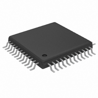
MAX1184ECM+TD Maxim Integrated Products, MAX1184ECM+TD Datasheet - Page 13

MAX1184ECM+TD
Manufacturer Part Number
MAX1184ECM+TD
Description
IC ADC 10BIT 20MSPS DL 48-TQFP
Manufacturer
Maxim Integrated Products
Datasheet
1.MAX1184ECMD.pdf
(21 pages)
Specifications of MAX1184ECM+TD
Number Of Bits
10
Sampling Rate (per Second)
20M
Data Interface
Parallel
Number Of Converters
2
Power Dissipation (max)
150mW
Voltage Supply Source
Single Supply
Operating Temperature
-40°C ~ 85°C
Mounting Type
Surface Mount
Package / Case
48-TQFP Exposed Pad, 48-eTQFP, 48-HTQFP, 48-VQFP
Lead Free Status / RoHS Status
Lead free / RoHS Compliant
The MAX1184’s CLK input accepts CMOS-compatible
clock signals. Since the interstage conversion of the
device depends on the repeatability of the rising and
falling edges of the external clock, use a clock with low
jitter and fast rise and fall times (< 2ns). In particular,
sampling occurs on the rising edge of the clock signal,
requiring this edge to provide lowest possible jitter. Any
significant aperture jitter would limit the SNR perfor-
mance of the on-chip ADCs as follows:
where f
is the time of the aperture jitter.
Clock jitter is especially critical for undersampling
applications. The clock input should always be consid-
ered as an analog input and routed away from any ana-
log input or other digital signal lines.
Figure 3. System Timing Diagram
ANALOG INPUT
Dual 10-Bit, 20Msps, 3V, Low-Power ADC with
DATA OUTPUT
DATA OUTPUT
CLOCK INPUT
IN
D9A–D0A
D9B–D0B
represents the analog input frequency and t
SNR
=
20
______________________________________________________________________________________
Internal Reference and Parallel Outputs
×
log
t
DO
⎛
⎜
⎝
2
× ×
N - 6
N - 6
π
Clock Input (CLK)
f
1
IN
N
×
t
AJ
N - 5
N - 5
)
⎞
⎟
⎠
N + 1
N - 4
N - 4
AJ
5-CLOCK-CYCLE LATENCY
N + 2
t
CH
The MAX1184 clock input operates with a voltage thresh-
old set to V
50%, must meet the specifications for high and low peri-
ods as stated in the Electrical Characteristics.
Figure 3 depicts the relationship between the clock
input, analog input, and data output. The MAX1184
samples at the rising edge of the input clock. Output
data for channels A and B is valid on the next rising
edge of the input clock. The output data has an internal
latency of five clock cycles. Figure 4 also determines
the relationship between the input clock parameters
and the valid output data on channels A and B.
All digital outputs, D0A–D9A (Channel A) and
D0B–D9B (Channel B), are TTL/CMOS logic-compati-
ble. There is a five-clock-cycle latency between any
particular sample and its corresponding output data.
N - 3
N - 3
Digital Output Data, Output Data Format
N + 3
Selection (T/B), Output Enable ( OE )
DD
N - 2
N - 2
/2. Clock inputs with a duty cycle other than
t
CL
System Timing Requirements
N + 4
N - 1
N - 1
N + 5
N
N
N + 6
N + 1
N + 1
13


