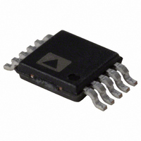
AD7685CRM Analog Devices Inc, AD7685CRM Datasheet - Page 14

AD7685CRM
Manufacturer Part Number
AD7685CRM
Description
IC ADC 16BIT PSEUDO-DIFF 10-MSOP
Manufacturer
Analog Devices Inc
Series
PulSAR®r
Datasheet
1.AD7685BCPZRL7.pdf
(28 pages)
Specifications of AD7685CRM
Design Resources
Parametric Measurement Unit and Supporting Components for PAD Appls Using AD5522 and AD7685 (CN0104) Integrated Device Power Supply for PAD with Output Voltage Range 0 V to 25 V (CN0130)
Number Of Bits
16
Sampling Rate (per Second)
250k
Data Interface
DSP, MICROWIRE™, QSPI™, Serial, SPI™
Number Of Converters
1
Power Dissipation (max)
15mW
Voltage Supply Source
Single Supply
Operating Temperature
-40°C ~ 85°C
Mounting Type
Surface Mount
Package / Case
10-TFSOP (0.118", 3.00mm Width)
For Use With
EVAL-AD7685CBZ - BOARD EVAL FOR AD7685
Lead Free Status / RoHS Status
Contains lead / RoHS non-compliant
Available stocks
Company
Part Number
Manufacturer
Quantity
Price
Part Number:
AD7685CRMZ
Manufacturer:
ADI/亚德诺
Quantity:
20 000
Part Number:
AD7685CRMZ-RL7
Manufacturer:
ADI/亚德诺
Quantity:
20 000
Part Number:
AD7685CRMZRL7
Manufacturer:
ADI/亚德诺
Quantity:
20 000
AD7685
Transfer Functions
The ideal transfer characteristic for the AD7685 is shown in
Figure 26 and Table 8.
Table 8. Output Codes and Ideal Input Voltages
Description
FSR – 1 LSB
Midscale + 1 LSB
Midscale
Midscale – 1 LSB
–FSR + 1 LSB
–FSR
1
2
This is also the code for an overranged analog input (V
This is also the code for an underranged analog input (V
000...010
000...001
000...000
111...101
111...111
111...110
–FS + 0.5 LSB
–FS
Figure 26. ADC Ideal Transfer Function
–FS + 1 LSB
0 TO VREF
NOTES
1. SEE VOLTAGE REFERENCE INPUT SECTION FOR REFERENCE SELECTION.
2. C
3. SEE DRIVER AMPLIFIER CHOICE SECTION.
4. OPTIONAL FILTER. SEE ANALOG INPUT SECTION.
5. SEE DIGITAL INTERFACE FOR MOST CONVENIENT INTERFACE MODE.
3
ANALOG INPUT
REF
≤–2V
≥7V
≥7V
IS USUALLY A 10µF CERAMIC CAPACITOR (X5R).
+FS – 1.5 LSB
REF
Analog Input V
4.999924 V
76.3 μV
0 V
2.500076 V
2.5 V
2.499924 V
4
2.7nF
IN+
33Ω
Figure 27. Typical Application Diagram with Multiple Supplies
1
− V
+FS – 1 LSB
IN+
IN−
− V
10µF
above V
IN−
2
below V
REF
IN+
IN–
REF
− V
= 5 V
GND
GND
Rev. B | Page 14 of 28
REF
GND
).
).
AD7685
VDD
VIO
TYPICAL CONNECTION DIAGRAM
Figure 27 shows an example of the recommended connection
diagram for the AD7685 when multiple supplies are available.
SCK
SDO
CNV
SDI
Digital Output Code Hexa
FFFF
8001
7FFF
0001
0000
8000
1
2
100nF
100nF
3- OR 4-WIRE INTERFACE
5V
1.8V TO VDD
5


