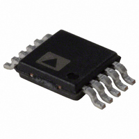
AD7685CRM Analog Devices Inc, AD7685CRM Datasheet - Page 22

AD7685CRM
Manufacturer Part Number
AD7685CRM
Description
IC ADC 16BIT PSEUDO-DIFF 10-MSOP
Manufacturer
Analog Devices Inc
Series
PulSAR®r
Datasheet
1.AD7685BCPZRL7.pdf
(28 pages)
Specifications of AD7685CRM
Design Resources
Parametric Measurement Unit and Supporting Components for PAD Appls Using AD5522 and AD7685 (CN0104) Integrated Device Power Supply for PAD with Output Voltage Range 0 V to 25 V (CN0130)
Number Of Bits
16
Sampling Rate (per Second)
250k
Data Interface
DSP, MICROWIRE™, QSPI™, Serial, SPI™
Number Of Converters
1
Power Dissipation (max)
15mW
Voltage Supply Source
Single Supply
Operating Temperature
-40°C ~ 85°C
Mounting Type
Surface Mount
Package / Case
10-TFSOP (0.118", 3.00mm Width)
For Use With
EVAL-AD7685CBZ - BOARD EVAL FOR AD7685
Lead Free Status / RoHS Status
Contains lead / RoHS non-compliant
Available stocks
Company
Part Number
Manufacturer
Quantity
Price
Part Number:
AD7685CRMZ
Manufacturer:
ADI/亚德诺
Quantity:
20 000
Part Number:
AD7685CRMZ-RL7
Manufacturer:
ADI/亚德诺
Quantity:
20 000
Part Number:
AD7685CRMZRL7
Manufacturer:
ADI/亚德诺
Quantity:
20 000
AD7685
CHAIN MODE, NO BUSY INDICATOR
This mode can be used to daisy-chain multiple AD7685s on a
3-wire serial interface. This feature is useful for reducing
component count and wiring connections, for example, in
isolated multiconverter applications or for systems with a
limited interfacing capacity. Data readback is analogous to
clocking a shift register.
A connection diagram example using two AD7685s is shown in
Figure 42, and the corresponding timing is given in Figure 43.
When SDI and CNV are low, SDO is driven low. With SCK low,
a rising edge on CNV initiates a conversion and selects the
chain mode. In this mode, CNV is held high during the
conversion phase and the subsequent data readback. When the
conversion is complete, the MSB is output onto SDO and the
SDO
ACQUISITION
SDI
A
t
HSCKCNV
= SDI
CNV
SCK
SDO
A
= 0
B
B
CONVERSION
t
SSCKCNV
t
CONV
t
EN
SDI
t
t
HSDO
DSDO
AD7685
CNV
SCK
A
D
D
1
A
B
15
15
t
SSDISCK
SDO
D
D
2
A
B
Figure 43. Chain Mode Serial Interface Timing
Figure 42. Chain Mode Connection Diagram
14
14
D
D
3
A
B
13
13
Rev. B | Page 22 of 28
t
SCKL
SDI
t
HSDISCK
14
AD7685
CNV
SCK
B
t
D
D
15
CYC
A
B
AD7685 enters the acquisition phase and powers down. The
remaining data bits stored in the internal shift register are then
clocked by subsequent SCK falling edges. For each ADC, SDI
feeds the input of the internal shift register and is clocked by the
SCK falling edge. Each ADC in the chain outputs its data MSB
first, and 16 × N clocks are required to readback the N ADCs.
The data is valid on both SCK edges. Although the rising edge
can be used to capture the data, a digital host using the SCK
falling edge will allow a faster reading rate and, consequently,
more AD7685s in the chain, provided the digital host has an
acceptable hold time. The maximum conversion rate may be
reduced due to the total readback time. For instance, with a 5 ns
digital host setup time and 3 V interface, up to eight AD7685s
running at a conversion rate of 220 kSPS can be daisy-chained
on a 3-wire port.
1
1
ACQUISITION
t
SDO
SCK
t
SCKH
t
D
D
ACQ
16
A
B
0
0
D
17
A
15
CONVERT
DATA IN
CLK
D
18
A
DIGITAL HOST
14
30
D
31
A
1
D
32
A
0


