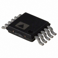
AD7685CRM Analog Devices Inc, AD7685CRM Datasheet - Page 3

AD7685CRM
Manufacturer Part Number
AD7685CRM
Description
IC ADC 16BIT PSEUDO-DIFF 10-MSOP
Manufacturer
Analog Devices Inc
Series
PulSAR®r
Datasheet
1.AD7685BCPZRL7.pdf
(28 pages)
Specifications of AD7685CRM
Design Resources
Parametric Measurement Unit and Supporting Components for PAD Appls Using AD5522 and AD7685 (CN0104) Integrated Device Power Supply for PAD with Output Voltage Range 0 V to 25 V (CN0130)
Number Of Bits
16
Sampling Rate (per Second)
250k
Data Interface
DSP, MICROWIRE™, QSPI™, Serial, SPI™
Number Of Converters
1
Power Dissipation (max)
15mW
Voltage Supply Source
Single Supply
Operating Temperature
-40°C ~ 85°C
Mounting Type
Surface Mount
Package / Case
10-TFSOP (0.118", 3.00mm Width)
For Use With
EVAL-AD7685CBZ - BOARD EVAL FOR AD7685
Lead Free Status / RoHS Status
Contains lead / RoHS non-compliant
Available stocks
Company
Part Number
Manufacturer
Quantity
Price
Part Number:
AD7685CRMZ
Manufacturer:
ADI/亚德诺
Quantity:
20 000
Part Number:
AD7685CRMZ-RL7
Manufacturer:
ADI/亚德诺
Quantity:
20 000
Part Number:
AD7685CRMZRL7
Manufacturer:
ADI/亚德诺
Quantity:
20 000
SPECIFICATIONS
VDD = 2.3 V to 5.5 V, VIO = 2.3 V to VDD, V
Table 2.
Parameter
RESOLUTION
ANALOG INPUT
ACCURACY
THROUGHPUT
AC ACCURACY
1
2
3
4
LSB means least significant bit. With the 5 V input range, 1 LSB is 76.3 μV.
See Terminology section. These specifications do include full temperature range variation but do not include the error contribution from the external reference.
All specifications in dB are referred to a full-scale input FS. Tested with an input signal at 0.5 dB below full-scale, unless otherwise specified.
f
IN1
Voltage Range
Absolute Input Voltage
Analog Input CMRR
Leakage Current at 25°C
Input Impedance
No Missing Codes
Differential Linearity Error
Integral Linearity Error
Transition Noise
Gain Error
Gain Error Temperature Drift
Offset Error
Offset Temperature Drift
Power Supply Sensitivity
Conversion Rate
Transient Response
Signal-to-Noise Ratio
Spurious-Free Dynamic
Total Harmonic Distortion
Signal-to-(Noise + Distortion)
Intermodulation Distortion
= 21.4 kHz, f
Range
2
2
, T
, T
IN2
MIN
MIN
= 18.9 kHz, each tone at −7 dB below full scale.
to T
to T
MAX
MAX
4
Conditions
IN+ − IN−
IN+
IN−
f
Acquisition phase
REF = VDD = 5 V
VDD = 4.5 V to 5.5 V
VDD = 2.3 V to 4.5 V
VDD = 5 V ± 5%
VDD = 4.5 V to 5.5 V
VDD = 2.3 V to 4.5 V
Full-scale step
f
V
f
V
f
f
f
V
f
V
−60 dB input
f
V
IN
IN
IN
IN
IN
IN
IN
IN
REF
REF
REF
REF
REF
= 250 kHz
= 20 kHz,
= 20 kHz,
= 20 kHz
= 20 kHz
= 20 kHz,
= 20 kHz,
= 20 kHz,
= 5 V
= 2.5 V
= 5 V
= 5 V,
= 2.5 V
REF
= VDD, T
Min
16
0
−0.1
−0.1
15
−6
0
0
Analog Inputs section
A
Rev. B | Page 3 of 28
= –40°C to +85°C, unless otherwise noted.
A Grade
Typ
65
1
0.5
±2
±0.3
±0.1
±0.7
±0.3
±0.05
90
86
−100
−100
89
86
See the
Max
V
VDD +
0.1
+0.1
+6
±30
±1.6
±3.5
200
1.8
250
REF
Min
16
0
−0.1
−0.1
16
−1
−3
0
90
86
90
85.5
0
Analog Inputs section
B Grade
Typ
65
1
±0.7
±1
0.5
±2
±0.3
±0.1
±0.7
±0.3
±0.05
92
88
−106
−106
92
32
87.5
−110
See the
Max
V
VDD +
0.1
+0.1
+3
±30
±1.6
±3.5
250
200
1.8
REF
Min
16
0
−0.1
−0.1
16
−1
−2
0
0
91.5
87.5
91.5
87
Analog Inputs section
C Grade
Typ
65
1
±0.5
±0.6
0.45
±2
±0.3
±0.1
±0.7
±0.3
±0.05
93.5
88.5
−110
−110
93.5
33.5
88.5
−115
See the
+0.1
+1.5
+2
±15
Max
V
VDD +
0.1
±1.6
±3.5
250
200
1.8
REF
AD7685
V
LSB
LSB
Unit
Bits
V
V
dB
nA
Bits
LSB
LSB
ppm/°C
mV
mV
ppm/°C
LSB
kSPS
kSPS
μs
dB
dB
dB
dB
dB
dB
dB
dB
3
1


