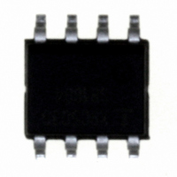
X9C503S Intersil, X9C503S Datasheet - Page 5

X9C503S
Manufacturer Part Number
X9C503S
Description
IC DIGITAL POT 50K 100TP 8SOIC
Manufacturer
Intersil
Series
XDCP™r
Datasheet
1.X9C503SIZT1.pdf
(10 pages)
Specifications of X9C503S
Taps
100
Resistance (ohms)
50K
Number Of Circuits
1
Temperature Coefficient
300 ppm/°C Typical
Memory Type
Non-Volatile
Interface
Up/Down (3-Wire)
Voltage - Supply
4.5 V ~ 5.5 V
Operating Temperature
0°C ~ 70°C
Mounting Type
Surface Mount
Package / Case
8-SOIC (3.9mm Width)
Resistance In Ohms
50K
Lead Free Status / RoHS Status
Contains lead / RoHS non-compliant
Available stocks
Company
Part Number
Manufacturer
Quantity
Price
Company:
Part Number:
X9C503S8IZ
Manufacturer:
Intersil
Quantity:
50
Part Number:
X9C503S8IZT1
Manufacturer:
INTERSIL
Quantity:
20 000
Company:
Part Number:
X9C503SI
Manufacturer:
XICOR
Quantity:
1 831
Part Number:
X9C503SI
Manufacturer:
INTELSIL
Quantity:
20 000
Company:
Part Number:
X9C503SIZ
Manufacturer:
Intersil
Quantity:
100
Part Number:
X9C503SIZ
Manufacturer:
INTERSIL
Quantity:
20 000
Company:
Part Number:
X9C503SIZT1
Manufacturer:
Intersil
Quantity:
2 500
Company:
Part Number:
X9C503SIZT1
Manufacturer:
Intersil
Quantity:
4 000
Part Number:
X9C503SIZT1
Manufacturer:
INTERSIL
Quantity:
20 000
Electrical Specifications
NOTES:
Endurance and Data Retention
AC Conditions of Test
Medium Endurance
Data Retention
Input Pulse Levels
Input Rise and Fall Times
Input Reference Levels
AC OPERATION CHARACTERISTICS
3. Absolute linearity is utilized to determine actual wiper voltage vs expected voltage = [V
4. Relative linearity is a measure of the error in step size between taps = V
5. 1 MI = Minimum Increment = R
6. Typical values are for T
7. This parameter is not 100% tested.
Test Circuit #1
SYMBOL
V
S
t
t
PARAMETER
t
t
IW
t
t
R
CPH
CPH
CYC
CYC
t
t
t
t
t
t
t
PU
Cl
lD
DI
lH
lC
, t
lL
(5)
F
CS to INC Setup
INC HIGH to U/D Change
U/D to INC Setup
INC LOW Period
INC HIGH Period
INC Inactive to CS Inactive
CS Deselect Time (STORE)
CS Deselect Time (NO STORE)
INC to V
INC Cycle Time
INC Input Rise and Fall Time
Power-up to Wiper Stable (Note 7)
V
CC
Power-up Rate (Note 7)
V
V
W/RW
A
R
L
/R
= +25°C and nominal supply voltage.
/R
L
H
100,000
Change
V
MIN
5
PARAMETER
100
w
TOT
Over recommended operating conditions unless otherwise stated. (Continued)
/R
TEST POINT
W
/99.
Data changes per bit
per register
years
X9C102, X9C103, X9C104, X9C503
0V to 3V
10ns
1.5V
UNIT
Test Circuit #2
V
V
H
L
/R
/R
TEST CONDITIONS
L
H
V
W
W(n + 1)
TEST POINT
/R
Power-up and Down Requirements
At all times, voltages on the potentiometer pins must be less
than ±V
memory is not in effect until the V
value. The V
w
FORCE
CURRENT
- [V
W(n)(actual)
CC
W(n) + MI
. The recall of the wiper position from non-volatile
CC
- V
] = +0.2 MI.
ramp rate specification is always in effect.
W(n)(expected )
Circuit #3 SPICE Macro Model
MIN
100
100
100
2.9
0.2
20
R
1
1
1
2
L
] = ±1 MI Maximum.
(Note 6)
LIMITS
TYP
10pF
100
500
C
L
CC
R
TOTAL
R
supply reaches its final
W
25pF
C
MAX
500
50
W
10pF
C
July 20, 2009
UNIT
V/ms
L
ms
ns
ns
µs
µs
µs
µs
ns
µs
µs
µs
µs
FN8222.3
R
H


