X9252WV24IZ-2.7 Intersil, X9252WV24IZ-2.7 Datasheet - Page 5
X9252WV24IZ-2.7
Manufacturer Part Number
X9252WV24IZ-2.7
Description
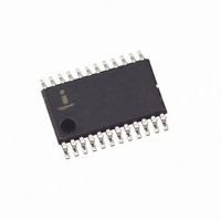
IC POT DGTL QUAD 24-TSSOP
Manufacturer
Intersil
Series
XDCP™r
Datasheet
1.X9252YV24IZ-2.7.pdf
(20 pages)
Specifications of X9252WV24IZ-2.7
Taps
256
Resistance (ohms)
10K
Number Of Circuits
4
Temperature Coefficient
300 ppm/°C Typical
Memory Type
Non-Volatile
Interface
I²C, 2-Wire Serial
Voltage - Supply
2.7 V ~ 5.5 V
Operating Temperature
-40°C ~ 85°C
Mounting Type
Surface Mount
Package / Case
24-TSSOP
Resistance In Ohms
10K
Track Taper
Linear
Resistance Tolerance
± 20%
No. Of Steps
256
Supply Voltage Range
2.7V To 5.5V
Control Interface
2 Wire, Serial
No. Of Pots
Quad
Rohs Compliant
Yes
Lead Free Status / RoHS Status
Lead free / RoHS Compliant
Available stocks
Company
Part Number
Manufacturer
Quantity
Price

Part Number:
X9252WV24IZ-2.7
Manufacturer:
INTERSIL
Quantity:
20 000


Endurance and Data Retention
Capacitance
2-Wire Interface timing (s)
Power-Up Timing
DC Electrical Specifications
A.C. Test Conditions
C
f
t
t
t
t
t
t
t
t
t
t
t
t
I
Input rise and fall times
Input and output timing threshold level
External load at pin SDA
SCL
HIGH
LOW
SU:STA
HD:STA
SU:STO
SU:DAT
HD:DAT
R
F
AA
DH
IN
nput Pulse Levels
SYMBOL
IN/OUT
t
C
D
SYMBOL
(Note 5)
(Note 5)
(Note 5)
IN
(Note 5)
SYMBOL
V
Symbol
(Notes 5, 9)
V
V
I
OL
L
IH
IL
(Note 5)
(Note 5) Input / Output capacitance (SDA)
Leakage current, bus interface pins
Input HIGH voltage
Input LOW voltage
SDA pin output LOW voltage
Minimum endurance
Clock Frequency
Clock High Time
Clock Low Time
Start Condition Setup Time
Start Condition Hold Time
Stop Condition Setup Time
SDA Data Input Setup Time
SDA Data Input Hold Time
SCL and SDA Rise Time
SCL and SDA Fall Time
SCL Low to SDA Data Output Valid Time
SDA Data Output Hold Time
Pulse Width Suppression Time at SCL and SDA inputs
PARAMETER
Data retention
Input capacitance (SCL, WP, DS0, DS1, CS, U/D, A2, A1 and
A0)
Power Up Delay from V
completed, and communication interfaces ready for operation.
PARAMETER
5
Over the recommended operating conditions unless otherwise specified. (Continued)
CC
power up (V
Test
PARAMETER
PARAMETER
Voltage at pin from V
I
OL
100,000
CC
MIN
100
= 3mA
above 2.7V) to wiper position recall
X9252
TEST CONDITIONS
SS
to V
Test Conditions
CC
V
V
OUT
IN
= 0V
= 0V
2.3kΩ to V
Data changes per bit
V
CC
1300
MIN
600
600
600
600
100
30
x 0.1 to V
UNITS
0
Years
CC
V
MAX
CC
10ns
V
and 100pF to V
2
CC
x 0.5
MIN
-10
Max.
-1
x 0.7
CC
8
6
x 0.9
MAX
400
300
300
0.9
50
V
V
CC
MAX
CC
0.4
10
SS
x 0.3
+ 1
November 14, 2005
UNITS
ms
Units
UNITS
pF
pF
UNITS
kHz
µs
ns
ns
ns
ns
ns
ns
ns
ns
ns
ns
ns
FN8167.2
µA
V
V
V
Related parts for X9252WV24IZ-2.7
Image
Part Number
Description
Manufacturer
Datasheet
Request
R

Part Number:
Description:
IC DCP QUAD 10K 256TAP 24-TSSOP
Manufacturer:
Intersil
Datasheet:

Part Number:
Description:
Intersil Corporation [CMOS Serial Controller Interface]
Manufacturer:
Intersil Corporation
Datasheet:
Part Number:
Description:
Manufacturer:
Intersil Corporation
Datasheet:
Part Number:
Description:
357-036-542-201 CARDEDGE 36POS DL .156 BLK LOPRO
Manufacturer:
Intersil Corporation
Datasheet:
Part Number:
Description:
1024-Word x 4-Bit LSI Static RAM
Manufacturer:
Intersil Corporation
Datasheet:
Part Number:
Description:
General Purpose NPN Transistor Arrays FN341.4
Manufacturer:
Intersil Corporation
Datasheet:
Part Number:
Description:
CMOS 16-Bit Microprocessor
Manufacturer:
Intersil Corporation
Datasheet:
Part Number:
Description:
Manufacturer:
Intersil Corporation
Datasheet:
Part Number:
Description:
Manufacturer:
Intersil Corporation
Datasheet:
Part Number:
Description:
Manufacturer:
Intersil Corporation
Datasheet:
Part Number:
Description:
Manufacturer:
Intersil Corporation
Datasheet:
Part Number:
Description:
CMOS 6-Bit Latch and Decoder Memory Interfaces
Manufacturer:
Intersil Corporation
Datasheet:
Part Number:
Description:
CA3046General Purpose NPN Transistor Arrays
Manufacturer:
Intersil Corporation
Datasheet:
Part Number:
Description:
Manufacturer:
Intersil Corporation
Datasheet:
Part Number:
Description:
TR909 DLC/FLC SLIC with Low Power Standby
Manufacturer:
Intersil Corporation
Datasheet: