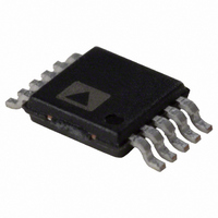
AD5170BRM50-RL7 Analog Devices Inc, AD5170BRM50-RL7 Datasheet - Page 15

AD5170BRM50-RL7
Manufacturer Part Number
AD5170BRM50-RL7
Description
IC DGTL POT 50K 256POS 10MSOP TR
Manufacturer
Analog Devices Inc
Datasheet
1.AD5170BRMZ50.pdf
(24 pages)
Specifications of AD5170BRM50-RL7
Rohs Status
RoHS non-compliant
Taps
256
Resistance (ohms)
50K
Number Of Circuits
1
Temperature Coefficient
35 ppm/°C Typical
Memory Type
Non-Volatile
Interface
I²C, 2-Wire Serial
Voltage - Supply
2.7 V ~ 5.5 V
Operating Temperature
-40°C ~ 125°C
Mounting Type
Surface Mount
Package / Case
10-MSOP, Micro10™, 10-uMAX, 10-uSOP
Resistance In Ohms
50K
The general equation that determines the digitally programmed
output resistance between Terminal W and Terminal B is
where:
D is the decimal equivalent of the binary code loaded in the
8-bit RDAC register.
R
R
the internal switch.
In summary, if R
the output resistance, R
shown in Table 7.
Table 7. Codes and Corresponding R
D (Dec)
255
128
1
0
Note that in the zero-scale condition, a finite wiper resistance of
100 Ω is present. Care should be taken to limit the current flow
between Terminal W and Terminal B in this state to a maximum
pulse current of no more than 20 mA. Otherwise, degradation
or possible destruction of the internal switch contact can occur.
Similar to the mechanical potentiometer, the resistance of the
RDAC between the wiper (Terminal W) and Terminal A also
produces a digitally controlled, complementary resistance, R
When these terminals are used, Terminal B can be opened.
Setting the resistance value for R
of resistance and decreases as the data loaded in the latch
increases in value. The general equation for this operation is
AB
W
is the wiper resistance contributed by the on resistance of
is the end-to-end resistance.
R
R
WB
WA
(D)
(D)
R
9961
5060
139
100
=
=
WB
128
256
SD BIT
D7
D6
D5
D4
D3
D2
D1
D0
(Ω)
DECODER
D
AB
128
LATCH
Figure 35. Equivalent RDAC Circuit
RDAC
AND
= 10 kΩ and Terminal A is open-circuited,
×
–
R
D
AB
WB
Output State
Full scale (R
Midscale
1 LSB
Zero scale (wiper contact resistance)
×
R
+
, is set for the RDAC latch codes, as
AB
2
×
R
R
R
R
+
S
S
S
S
R
2
W
WA
×
R
AB
starts at a maximum value
W
− 1 LSB + R
WB
Resistance
A
W
B
W
)
WA
Rev. F | Page 15 of 24
(1)
(2)
.
For R
some examples of the output resistance (R
latch codes.
Table 8. Codes and Corresponding R
D (Dec)
255
128
1
0
Typical device-to-device matching is process-lot dependent
and can vary by up to ±30%. Because the resistance element is
processed using thin film technology, the change in R
temperature has a very low 35 ppm/°C temperature coefficient.
PROGRAMMING THE POTENTIOMETER DIVIDER—
VOLTAGE OUTPUT OPERATION
The digital potentiometer easily generates a voltage divider at
wiper to B and wiper to A proportional to the input voltage at
A to B. Unlike the polarity of V
positive, voltage across A to B, W to A, and W to B can be at
either polarity.
If ignoring the effect of the wiper resistance for approximation,
connecting Terminal A to 5 V and Terminal B to ground pro-
duces an output voltage at the wiper to B starting at 0 V up to
1 LSB less than 5 V. Each LSB of voltage is equal to the voltage
applied across Terminal A and Terminal B divided by the 256
positions of the potentiometer divider. The general equation
defining the output voltage at V
valid input voltage applied to Terminal A and Terminal B is
For a more accurate calculation, which includes the effect of
wiper resistance, V
Operation of the digital potentiometer in divider mode results
in a more accurate operation over temperature. Unlike rheostat
mode, the output voltage is dependent mainly on the ratio of
the internal resistors, R
Therefore, the temperature drift reduces to 15 ppm/°C.
V
V
AB
W
W
= 10 kΩ and Terminal B open circuited, Table 8 shows
(
(
D
D
)
)
=
=
Figure 36. Potentiometer Mode Configuration
256
R
D
WB
R
R
139
5060
9961
10,060
AB
V
W
(
WA
D
A
, the following equation can be used:
V
)
+
(Ω)
I
V
WA
256
A
and R
256
+
−
R
A
B
D
WA
R
DD
W
WB
V
AB
W
(
D
with respect to ground for any
B
to GND, which must be
, and not the absolute values.
)
Output State
Full scale
Midscale
1 LSB
Zero scale
V
B
WA
V
O
Resistance
WA
) vs. the RDAC
AD5170
AB
with
(3)
(4)


