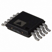
AD5170BRM50-RL7 Analog Devices Inc, AD5170BRM50-RL7 Datasheet - Page 21

AD5170BRM50-RL7
Manufacturer Part Number
AD5170BRM50-RL7
Description
IC DGTL POT 50K 256POS 10MSOP TR
Manufacturer
Analog Devices Inc
Datasheet
1.AD5170BRMZ50.pdf
(24 pages)
Specifications of AD5170BRM50-RL7
Rohs Status
RoHS non-compliant
Taps
256
Resistance (ohms)
50K
Number Of Circuits
1
Temperature Coefficient
35 ppm/°C Typical
Memory Type
Non-Volatile
Interface
I²C, 2-Wire Serial
Voltage - Supply
2.7 V ~ 5.5 V
Operating Temperature
-40°C ~ 125°C
Mounting Type
Surface Mount
Package / Case
10-MSOP, Micro10™, 10-uMAX, 10-uSOP
Resistance In Ohms
50K
After all the data bits are read or written, a stop condition is
established by the master. A stop condition is defined as a low-
to-high transition on the SDA line while SCL is high. In write
mode, the master pulls the SDA line high during the 10th clock
pulse to establish a stop condition (see Figure 45).
In read mode, the master issues a no acknowledge for the 9th
clock pulse (that is, the SDA line remains high). The master brings
the SDA line low before the 10th clock pulse and then brings the
SDA line high to establish a stop condition (see Figure 46).
A repeated write function gives the user flexibility to update the
RDAC output a number of times after addressing and instructing
the part only once. For example, after the RDAC has acknowledged
its slave address and instruction bytes in write mode, the RDAC
output updates on each successive byte. If different instructions
are needed, the write/read mode has to start again with a new
slave address, instruction, and data byte. Similarly, a repeated
read function of the RDAC is also allowed.
Multiple Devices on One Bus
Figure 47 shows four AD5170s on the same serial bus. Each has
a different slave address because the states of their AD0 and
AD1 pins are different, which allows each device on the bus to
be written to or read from independently. The master device
output bus line drivers are open-drain pull-downs in a fully
I
2
C-compatible interface.
Rev. F | Page 21
of 24
LEVEL SHIFTING FOR DIFFERENT VOLTAGE
OPERATION
If the SCL and SDA signals come from a low voltage logic con-
troller and are below the minimum V
shift the signals for read/write communications between the
AD5170 and the controller. Figure 48 shows one of the implemen-
tations. For example, when SDA1 is at 2.5 V, M1 turns off and
SDA2 becomes 5 V. When the SDA1 is at 0 V, M1 turns on and
the SDA2 approaches 0 V. As a result, proper level shifting is
established. M1 and M2 should be low threshold, N-channel
power MOSFETs, such as the FDV301N.
SDA1
SCL1
MASTER
V
DD1
CONTROLLER
= 2.5V
SDA
AD5170
Figure 48. Level Shifting for Different Voltage Operation
AD1
AD0
2.5V
R
SCL
P
Figure 47. Multiple AD5170s on One I
Rp
R
P
5V
SDA
AD5170
AD1
AD0
Rp
S
M1
SCL
G
5V
5V
D
S
M2
SDA
G
AD5170
AD1
AD0
IH
level (0.7 V × V
D
SCL
Rp
2
5V
C Bus
2.7V TO 5.5V
AD5170
SDA
Rp
AD5170
AD1
AD0
AD5170
V
SCL
DD2
DD
), level
= 5V
SDA
SCL
SDA2
SCL2


