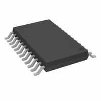
AD5233BRUZ50-R7 Analog Devices Inc, AD5233BRUZ50-R7 Datasheet - Page 23

AD5233BRUZ50-R7
Manufacturer Part Number
AD5233BRUZ50-R7
Description
IC DGTL POT QUAD 64POS 24-TSSOP
Manufacturer
Analog Devices Inc
Datasheet
1.AD5233BRUZ10-R7.pdf
(32 pages)
Specifications of AD5233BRUZ50-R7
Taps
64
Resistance (ohms)
50K
Number Of Circuits
4
Temperature Coefficient
600 ppm/°C Typical
Memory Type
Non-Volatile
Interface
4-Wire SPI Serial
Voltage - Supply
2.7 V ~ 5.5 V, ±2.25 V ~ 2.75 V
Operating Temperature
-40°C ~ 85°C
Mounting Type
Surface Mount
Package / Case
24-TSSOP
Resistance In Ohms
50K
Number Of Elements
4
# Of Taps
64
Resistance (max)
50KOhm
Power Supply Requirement
Single/Dual
Interface Type
Serial (4-Wire/SPI)
Single Supply Voltage (typ)
3/5V
Dual Supply Voltage (typ)
±2.5V
Single Supply Voltage (min)
2.7V
Single Supply Voltage (max)
5.5V
Dual Supply Voltage (min)
±2.25V
Dual Supply Voltage (max)
±2.75V
Operating Temp Range
-40C to 85C
Operating Temperature Classification
Industrial
Mounting
Surface Mount
Pin Count
24
Lead Free Status / RoHS Status
Lead free / RoHS Compliant
APPLICATIONS INFORMATION
BIPOLAR OPERATION FROM DUAL SUPPLIES
The AD5233 can be operated from dual supplies ±2.5 V, which
enables control of ground-referenced ac signals or bipolar opera-
tion. AC signals as high as V
across Terminal A and Terminal B with output taken from
Terminal W. See Figure 46 for a typical circuit connection.
GAIN CONTROL COMPENSATION
A digital potentiometer is commonly used in gain control such
as the noninverting gain amplifier shown in Figure 47.
When RDAC B terminal parasitic capacitance is connected
to the op amp noninverting node, it introduces a 0 for the
1/b
−20 dB/dec characteristics. A large R2 and finite C1 can cause
this zero’s frequency to fall well below the crossover frequency.
Therefore, the rate of closure becomes 40 dB/dec, and the
system as a 0° phase margin at the crossover frequency. The
output can ring or oscillate if an input is a rectangular pulse or
step function. Similarly, it is also likely to ring when switching
between two gain values; this is equivalent to a stop change at
the input.
Depending on the op amp GBP, reducing the feedback
resistor might extend the zero’s frequency far enough to
overcome the problem. A better approach is to include a
compensation capacitor, C2, to cancel the effect caused by
C1. Optimum compensation occurs when R1 × C1 = R2 ×
C2. This is not an option because of the variation of R2.
O
CONVERTER
term with 20 dB/dec, while a typical op amp GBP has
MICRO-
V
GND
DD
Figure 46. Bipolar Operation from Dual Supplies
Figure 47. Typical Noninverting Gain Amplifier
SCLK
33.2kΩ
MOSI
R1
SS
35pF
C1
V
AD5233
CS
CLK
SDI
GND
i
DD
/V
SS
10pF
U1
C2
V
V
can be applied directly
SS
DD
W
100kΩ
B
A
B
W
R2
±1.25V p-p
A
D = MIDSCALE
V
O
± 2.5V p-p
+2.5V
–2.5V
Rev. B | Page 23 of 32
As a result, one can use the previous relationship and scale C2
as if R2 were at its maximum value. Doing this might over-
compensate and compromise the performance when R2 is
set at low values. On the other hand, it avoids the ringing or
oscillation at the worst case. For critical applications, C2 should
be found empirically to suit the need. In general, C2 in the
range of picofarads is usually adequate for the compensation.
Similarly, W and A terminal capacitances are connected to the
output (not shown); their effect at this node is less significant
and the compensation can be avoided in most cases.
HIGH VOLTAGE OPERATION
The digital potentiometer can be placed directly in the feedback
or input path of an op amp for gain control, provided that the
voltage across Terminal A and Terminal B, Terminal W and
Terminal A, or Terminal W and Terminal B does not exceed
|5 V|. When high voltage gain is needed, users should set a
fixed gain in an op amp operated at high voltage and let the
digital potentiometer control the adjustable input. Figure 48
shows a simple implementation.
Similarly, a compensation capacitor, C, might be needed to
dampen the potential ringing when the digital potentiometer
changes steps. This effect is prominent when stray capacitance
at the inverted node is augmented by a large feedback resistor.
Usually, a capacitor (C) of a few picofarads, is adequate to combat
the problem.
DAC
Figure 49 shows a unipolar 8-bit DAC using the AD5233. The
buffer is needed to drive various loads.
1
2
AD5233
5V
GND
V
IN
U1
V
AD1582
OUT
Figure 48. 5 V Voltage Span Control
Figure 49. Unipolar 8-Bit DAC
3
5V
A
B
AD5233
W
R
A
B
W
A1
AD8601
–
+
A2
V+
V–
2R
15V
V+
V–
5V
C
0 TO 15V
V
V
O
O
AD5233


