ISL22317UFRTZ-TK Intersil, ISL22317UFRTZ-TK Datasheet - Page 10

ISL22317UFRTZ-TK
Manufacturer Part Number
ISL22317UFRTZ-TK
Description
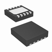
IC POT DGTL 128TP LN LP 10-TDFN
Manufacturer
Intersil
Series
XDCP™r
Datasheet
1.ISL22317TFRTZ-TK.pdf
(15 pages)
Specifications of ISL22317UFRTZ-TK
Taps
128
Resistance (ohms)
50K
Number Of Circuits
1
Memory Type
Non-Volatile
Interface
I²C, 2-Wire Serial
Voltage - Supply
2.7 V ~ 5.5 V
Operating Temperature
-40°C ~ 125°C
Mounting Type
Surface Mount
Package / Case
10-TDFN Exposed Pad
Resistance In Ohms
50K
Lead Free Status / RoHS Status
Lead free / RoHS Compliant
Temperature Coefficient
-
Available stocks
Company
Part Number
Manufacturer
Quantity
Price
Company:
Part Number:
ISL22317UFRTZ-TK
Manufacturer:
Intersil
Quantity:
50
Typical Performance Curves
Pin Description
Potentiometers Pins
RH AND RL
The high (RH) and low (RL) terminals of the ISL22317 are
equivalent to the fixed terminals of a mechanical
potentiometer. RH and RL are referenced to the relative
position of the wiper and the voltage potential on the
terminals. With WR set to 127 decimal, the wiper will be
closest to RH. With the WR set to 0, the wiper is closest to
RL. The voltage potential on the RH terminal must be higher
than voltage potential on RL terminal.
RW
RW is the wiper terminal and is equivalent to the movable
terminal of a mechanical potentiometer. The position of the
wiper within the array is determined by the WR register.
REF_A, REF_B
REF_A and REF_B are pins to connect an external resistor.
If application is required to connect RL terminal to GND, then
the REF_B pin should also be connected to GND.
FIGURE 17. TC FOR RHEOSTAT MODE (10k/50k/100k) IN ppm
800
600
400
200
40
30
20
10
0
15
0
-40
FIGURE 19. STANDBY I
V
CC
[R
35
REF
= 5.5V
V
CC
0
2ppm/°C]
= 5.5V
TAP POSITION (DECIMAL)
55
TEMPERATURE (°C)
V
CC
10
= 2.7V
V
CC
CC
40
= 2.7V
75
vs TEMPERATURE
(Continued)
95
80
115
120
ISL22317
Warning! Do not connect REF_A to GND under any
circumstances. That may damage the ISL22317.
Bus Interface Pins
SERIAL DATA INPUT/OUTPUT (SDA)
The SDA is a bidirectional serial data input/output pin for I
interface. It receives device address, operation code, wiper
address and data from an I
rising edge of the serial clock SCL, and it shifts out data after
each falling edge of the serial clock.
SDA requires an external pull-up resistor, since it is an open
drain input/output.
SERIAL CLOCK (SCL)
This input is the serial clock of the I
DEVICE ADDRESS (A1)
The address input is used to set the A1 bit of the 7-bit I
interface slave address, see Table 4. A match in the slave
address serial data stream must match with the Address
input pins in order to initiate communication with the
FIGURE 18. TC FOR VOLTAGE DIVIDER MODE (10k/50k/100k)
FIGURE 20. WIPER RESISTANCE vs TAP POSITION WHEN
100
40
30
20
10
80
60
40
20
0
0
15
0
V
IN ppm [R
PRECISION IS OFF
CC
20
35
= 5.5V
TAP POSITION (DECIMAL)
TAP POSITION (DECIMAL)
40
REF
55
2
10ppm/°C]
T = +25°C
C external master device at the
60
V
CC
75
2
T = +125°C
C serial interface.
= 2.7V
80
95
T = -40°C
V
100
CC
= 5.5V
April 15, 2010
115
FN6912.1
2
120
C
2
C


