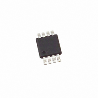
ISL90810UIU8Z Intersil, ISL90810UIU8Z Datasheet - Page 5

ISL90810UIU8Z
Manufacturer Part Number
ISL90810UIU8Z
Description
IC POT DGTL 50K OHM 8-MSOP
Manufacturer
Intersil
Series
XDCP™r
Datasheet
1.ISL90810UIU8Z-TK.pdf
(11 pages)
Specifications of ISL90810UIU8Z
Taps
256
Resistance (ohms)
50K
Number Of Circuits
1
Temperature Coefficient
35 ppm/°C Typical
Memory Type
Volatile
Interface
I²C, 2-Wire Serial
Voltage - Supply
2.7 V ~ 5.5 V
Operating Temperature
-40°C ~ 85°C
Mounting Type
Surface Mount
Package / Case
8-MSOP, Micro8™, 8-uMAX, 8-uSOP,
Resistance In Ohms
50K
Lead Free Status / RoHS Status
Lead free / RoHS Compliant
Available stocks
Company
Part Number
Manufacturer
Quantity
Price
Company:
Part Number:
ISL90810UIU8Z
Manufacturer:
Intersil
Quantity:
48
Operating Specifications
SDA vs SCL Timing
NOTES:
10. Roffset = R
12. RINL = [R
13.
14. This parameter is not 100% tested.
11. RDNL = (R
2. Typical values are for T
3. LSB: [V(RW)
4. ZS error = V(RW)
5. FS error = [V(RW)
6. DNL = [V(RW)
7. INL = (V(RW)
8.
9. MI =
Rpu (Note 14) SDA and SCL Bus Pull-Up Resistor
t
Cb (Note 14)
DH
t
t
R
F
(OUTPUT TIMING)
SYMBOL
(INPUT TIMING)
t
incremental voltage when changing from one tap to an adjacent tap.
Roffset = R
TC
TC
HD:STO
(Note 14)
(Note 14)
(Note 14)
V
R
|
R
=
=
255
--------------------------------------------------------------------------------------------- -
[
--------------------------------------------------------------- -
[
Max V RW
Max Ri
i
[
SDA
SCL
Max V RW
– (MI • i) – R
Max Ri
i
0
255
– R
SDA
– R
/MI, when measuring between RW and RL.
255
STOP Condition Hold Time for Read,
or Volatile Only Write
Output Data Hold Time
SDA and SCL Rise Time
SDA and SCL Fall Time
Capacitive Loading of SDA or SCL
Off-Chip
i
(
(
i
t
– i • LSB – V(RW)
/MI, when measuring between RW and RH.
0
SU:STA
– V(RW)
(
i-1
(
|/
(
– V(RW)
0
255. R
)
)/MI, for i = 32 to 255.
255
(
/LSB.
+
) Min Ri
–
Min Ri
)
– V
i
)
)
A
0
i
i-1
255
+
) Min V RW
]/MI, for i = 32 to 255.
(
PARAMETER
= +25°C and 3.3V supply voltage.
0
CC
–
Min V RW
(
]/LSB-1, for i = 1 to 255. i is the DCP register setting.
]/255. V(RW)
and R
)
t
]/LSB.
HD:STA
] 2 ⁄
5
)
(
]
Over the recommended operating conditions unless otherwise specified. (Continued)
(
0
(
×
)/LSB, for i = 1 to 255.
(
0
---------------- -
145°C
are the measured resistances for the DCP register set to FF hex and 00 hex respectively.
10
)
t
i
F
6
)
255
)
i
] 2 ⁄
)
t
SU:DAT
for i = 32 to 255, T = -40°C to +105°C. Max( ) is the maximum value of the resistance and Min ( ) is the
minimum value of the resistance over the temperature range.
and V(RW)
×
---------------- -
145°C
10
6
From SDA rising edge to SCL falling edge. Both
crossing 70% of V
From SCL falling edge crossing 30% of V
SDA enters the 30% to 70% of V
From 30% to 70% of V
From 70% to 30% of V
Total on-chip and off-chip
Maximum is determined by t
For Cb = 400pF, max is about 2~2.5kΩ.
For Cb = 40pF, max is about 15~20kΩ
t
HIGH
0
for i = 16 to 240 decimal, T = -40°C to +105°C. Max( ) is the maximum value of the wiper
voltage and Min ( ) is the minimum value of the wiper voltage over the temperature range.
are V(RW) for the DCP register set to FF hex and 00 hex respectively. LSB is the
ISL90810
t
TEST CONDITIONS
LOW
CC
t
HD:DAT
.
CC
CC
R
and t
t
CC
R
F
window.
.
t
AA
CC
, until
t
DH
0.1 * Cb
0.1 * Cb
20 +
20 +
MIN
600
10
0
1
(Note 1)
t
TYP
BUF
t
SU:STO
MAX
250
250
400
November 10, 2006
UNITS
FN8234.2
pF
kΩ
ns
ns
ns
ns


