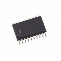
X9221AYSIZ Intersil, X9221AYSIZ Datasheet

X9221AYSIZ
Specifications of X9221AYSIZ
Related parts for X9221AYSIZ
X9221AYSIZ Summary of contents
Page 1
... CAUTION: These devices are sensitive to electrostatic discharge; follow proper IC Handling Procedures. | 1-888-INTERSIL or 1-888-468-3774 Intersil (and design registered trademark of Intersil Americas Inc. XDCP is a trademark of Intersil Americas Inc. Copyright Intersil Americas Inc. 2005-2006. All Rights Reserved All other trademarks mentioned are the property of their respective owners. X9221A 64 Taps, 2-Wire Serial Bus FN8163 ...
Page 2
... Ordering Information PART NUMBER PART MARKING X9221AYS X9221AYS X9221AYSZ (Note) X9221AYS Z X9221AYSI* X9221AYSI X9221AYSIZ* (Note) X9221AYSI Z X9221AWS* X9221AWS X9221AWSZ* (Note) X9221AWS Z X9221AWSI* X9221AWSI X9221AWSIZ* (Note) X9221AWSI Z X9221AUP X9221AUP X9221AUPZ (Note) X9221AUPZ X9221AUPI X9221AUPI X9221AUPIZ (Note) X9221AUPIZ X9221AUSI* X9221AUSI X9221AUSIZ* (Note) X9221AUSI Z *Add " ...
Page 3
PIN NAMES Symbol Description SCL Serial Clock SDA Serial Data A0–A3 Address Potentiometers (terminal equivalent Potentiometers ...
Page 4
The next four bits of the slave address are the device address. The physical device address is defined by the state of the A0-A3 inputs. The X9221A compares the serial data stream with the address input state; a successful compare ...
Page 5
For each SCL clock pulse (t ) while SDA is HIGH, the selected wiper will HIGH move one resistor segment towards the V nal. Similarly, for each SCL clock pulse while SDA is Figure 3. ...
Page 6
Figure 6. Increment/Decrement Timing Limits INC/DEC CMD Issued SCL SDA Table 1. Instruction Set Instruction Read WCR 1 0 Write WCR 1 0 Read Data Register 1 0 Write Data Register 1 ...
Page 7
Figure 7. Acknowledge Response from Receiver SCL from Master Data Output from Transmitter Data Output from Receiver START DETAILED OPERATION Both XDCP potentiometers share the serial interface and share a common architecture. Each potentiometer is comprised of a resistor array, ...
Page 8
Figure 8. Detailed Potentiometer Block Diagram Serial Data Path From Interface Circuitry Register 0 Register 2 If WCR = 00[H] then WCR = 3F[H] then ...
Page 9
ABSOLUTE MAXIMUM RATINGS Temperature Under Bias ................... -65°C to +135°C Storage Temperature ........................ -65°C to +150°C Voltage on SCK, SCL or Any Address Input With Respect to V ...................... -1V to +7V SS Voltage on Any ...
Page 10
D.C. OPERATING CHARACTERISTICS (Over recommended operating conditions unless otherwise stated.) Symbol Parameter l Supply Current (Active Current (Standby Input Leakage Current LI I Output Leakage Current LO V Input HIGH Voltage IH V Input ...
Page 11
A.C. CONDITIONS OF TEST Input pulse levels V CC Input rise and fall times 10ns Input and output timing levels V CC SYMBOL TABLE WAVEFORM INPUTS Must be steady May change from LOW to HIGH May change from HIGH to ...
Page 12
A.C. CHARACTERISTICS (Over recommended operating conditions unless otherwise stated) Symbol f SCL clock frequency SCL t Clock LOW period LOW t Clock HIGH period HIGH t SCL and SDA rise time R t SCL and SDA fall time F T ...
Page 13
Figure 12. Start Stop Timing SCL t SU:STA SDA (Data in) Figure 13. Write Cycle and Wiper Response Timing SCL Clock 8 SDA SDA IN Wiper Output 13 X9221A START Condition t HD:STA Clock 9 STOP ACK STOP Condition t ...
Page 14
Small Outline Package Family (SO PIN #1 I.D. MARK 0.010 SEATING PLANE 0.004 C 0.010 MDP0027 SMALL OUTLINE PACKAGE FAMILY (SO) SYMBOL SO-8 SO-14 ...
Page 15
... Accordingly, the reader is cautioned to verify that data sheets are current before placing orders. Information furnished by Intersil is believed to be accurate and reliable. However, no responsibility is assumed by Intersil or its subsidiaries for its use; nor for any infringements of patents or other rights of third parties which may result from its use ...


