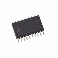
X9241AMS Intersil, X9241AMS Datasheet - Page 5

X9241AMS
Manufacturer Part Number
X9241AMS
Description
IC XDCP QUAD 2/10/10/50K 20-S
Manufacturer
Intersil
Series
XDCP™r
Datasheet
1.X9241AUP.pdf
(16 pages)
Specifications of X9241AMS
Taps
64
Resistance (ohms)
2K, 10K, 10K, 50K
Number Of Circuits
4
Temperature Coefficient
30 ppm/°C Typical
Memory Type
Non-Volatile
Interface
I²C, 2-Wire Serial
Voltage - Supply
4.5 V ~ 5.5 V
Operating Temperature
0°C ~ 70°C
Mounting Type
Surface Mount
Package / Case
20-SOIC (7.5mm Width)
Resistance In Ohms
2K, 10K, 10K, 50K
Lead Free Status / RoHS Status
Contains lead / RoHS non-compliant
Flow 1. ACK Polling Sequence
Instruction Structure
The next byte sent to the X9241A contains the instruction
and register pointer information. The 4 most significant bits
are the instruction. The next 4-bits point to one of four pots
and when applicable they point to one of four associated
registers. The format is in Figure 2.
COMMAND COMPLETED
NONVOLATILE WRITE
ENTER ACK POLLING
I3
ISSUE SLAVE
INSTRUCTION
OPERATION?
FIGURE 2. INSTRUCTION BYTE FORMAT
RETURNED?
INSTRUCTIONS
ADDRESS
FURTHER
PROCEED
SDA
ISSUE
START
SCL
ISSUE
ACK
I2
YES
YES
I1
S
T
A
R
T
NO
I0
0
POTENTIOMETER
NO
5
1
SELECT
P1
0
P0
1
FIGURE 3. TWO-BYTE INSTRUCTION SEQUENCE
ISSUE STOP
ISSUE STOP
REGISTER
R1
PROCEED
SELECT
A3
A2
R0
A1
A0
X9241A
A
C
K
I3
The 4 high order bits define the instruction. The next 2-bits
(P1 and P0) select which one of the four potentiometers is to
be affected by the instruction. The last 2-bits (R1 and R0)
select one of the four registers that are to be acted upon
when a register oriented instruction is issued.
Four of the nine instructions end with the transmission of the
instruction byte. The basic sequence is illustrated in Figure 3.
These two-byte instructions exchange data between the WCR
and one of the data registers. A transfer from a Data Register
to a WCR is essentially a write to a static RAM. The response
of the wiper to this action will be delayed t
from WCR current wiper position to a Data Register is a write
to nonvolatile memory and takes a minimum of t
complete. The transfer can occur between one of the four
potentiometers and one of its associated registers; or it may
occur globally, wherein the transfer occurs between all four of
the potentiometers and one of their associated registers.
Four instructions require a three-byte sequence to complete.
These instructions transfer data between the host and the
X9241A; either between the host and one of the Data
Registers or directly between the host and the WCR. These
instructions are: Read WCR, read the current wiper position
of the selected pot; Write WCR, change current wiper
position of the selected pot; Read Data Register, read the
contents of the selected nonvolatile register; Write Data
Register, write a new value to the selected Data Register.
The sequence of operations is shown in Figure 4.
The Increment/Decrement command is different from the
other commands. Once the command is issued and the
X9241A has responded with an acknowledge, the master
can clock the selected wiper up and/or down in one segment
steps; thereby, providing a fine tuning capability to the host.
For each SCL clock pulse (t
selected wiper will move one resistor segment towards the
V
SDA is LOW, the selected wiper will move one resistor
segment towards the V
of the sequence and timing for this operation is shown in
Figures 5 and 6 respectively.
H
I2
/R
H
I1
terminal. Similarly, for each SCL clock pulse while
I0
P1
P0
L
/R
R1
L
HIGH
terminal. A detailed illustration
R0
) while SDA is HIGH, the
A
C
K
S
O
P
T
STPWV
WR
. A transfer
August 31, 2007
to
FN8164.6


