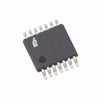
X9111TV14Z-2.7 Intersil, X9111TV14Z-2.7 Datasheet - Page 10

X9111TV14Z-2.7
Manufacturer Part Number
X9111TV14Z-2.7
Description
IC XDCP SGL 1024TAP 100K 14TSSOP
Manufacturer
Intersil
Series
XDCP™r
Datasheet
1.X9111TV14.pdf
(17 pages)
Specifications of X9111TV14Z-2.7
Taps
1024
Resistance (ohms)
100K
Number Of Circuits
1
Temperature Coefficient
300 ppm/°C Typical
Memory Type
Non-Volatile
Interface
SPI, 3-Wire Serial
Voltage - Supply
2.7 V ~ 5.5 V
Operating Temperature
0°C ~ 70°C
Mounting Type
Surface Mount
Package / Case
14-TSSOP
Resistance In Ohms
100K
Lead Free Status / RoHS Status
Lead free / RoHS Compliant
Available stocks
Company
Part Number
Manufacturer
Quantity
Price
Company:
Part Number:
X9111TV14Z-2.7
Manufacturer:
Intersil
Quantity:
1 425
Part Number:
X9111TV14Z-2.7
Manufacturer:
INTERSIL
Quantity:
20 000
A.C. Test Conditions
D.C. Operating Characteristics
Endurance And Data Retention
Capacitance
Power-Up Timing
NOTES:
I
Input rise and fall times
Input and output timing level
C
nput pulse levels
6. This parameter is not 100% tested.
7. t
SYMBOL
C
t
IN/OUT
t
r
t
C
PUW
PUR
OUT
I
I
V
parameters are not 100% tested.
V
V
V
SYMBOL
CC1
CC2
I
I
V
PUR
V
IN
SYMBOL
I
SB
LO
CC
LI
OL
OL
OL
IH
IL
(Note 6)
(Note 7)
(Note 6)
(Note 7)
(Note 6)
and t
(Note 6) Input/Output capacitance (SI)
V
(active)
V
(nonvolatile write)
V
Input leakage current
Output leakage current
Input HIGH voltage
Input LOW voltage
Output LOW voltage
Output LOW voltage
Output LOW voltage
Minimum Endurance
PUW
CC
CC
CC
Data Retention
PARAMETER
supply current
supply current
current (standby)
are the delays required from the time the (last) power supply (V
Output capacitance (SO)
Input capacitance (A0, CS, WP, HOLD, and SCK)
V
Power-up to initiation of read operation
Power-up to initiation of write operation
CC
PARAMETER
power-up rate
10
Over the recommended operating conditions unless otherwise specified.
PARAMETER
V
CC
x 0.1 to V
f
Other Inputs = V
f
Other Inputs = V
SCK = SI = V
CS = V
V
V
I
I
I
V
SCK
SCK
OL
OH
OH
IN
OUT
CC
TEST
10ns
= 3mA
= V
= -1mA, V
= -0.4mA, V
x 0.5
= 2.5 MHz, SO = Open, V
= 2.5MHz, SO = Open, V
= V
CC
SS
CC
100,000
SS
= 5.5V
to V
MIN
100
x 0.9
to V
SS
CC
TEST CONDITIONS
CC
, Addr. = V
CC
SS
SS
CC
≥ +3V
≤ +3V
X9111
SS
,
CC
CC
= 5.5V
CC
= 5.5V
MIN
-) is stable until the specific instruction can be issued. These
0.2
TEST CONDITIONS
Data changes per bit per register
V
V
V
OUT
OUT
IN
= 0V
V
V
V
= 0V
= 0V
CC
CC
CC
MIN.
-1
x 0.7
- 0.8
- 0.4
UNITS
years
MAX
50
50
1
TYP.
1
MAX
8
8
6
V
V
CC
MAX.
CC
400
0.4
10
10
5
3
x 0.3
+ 1
September 15, 2006
UNITS
V/ms
ms
ms
UNITS
pF
pF
pF
UNITS
FN8159.4
mA
µA
µA
µA
µA
V
V
V
V
V


