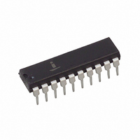
X9241AYPIZ Intersil, X9241AYPIZ Datasheet - Page 11

X9241AYPIZ
Manufacturer Part Number
X9241AYPIZ
Description
IC XDCP QUAD 4X2K EE 20-DIP
Manufacturer
Intersil
Series
XDCP™r
Datasheet
1.X9241AUP.pdf
(16 pages)
Specifications of X9241AYPIZ
Taps
64
Resistance (ohms)
2K
Number Of Circuits
4
Temperature Coefficient
30 ppm/°C Typical
Memory Type
Non-Volatile
Interface
I²C, 2-Wire Serial
Voltage - Supply
4.5 V ~ 5.5 V
Operating Temperature
-40°C ~ 85°C
Mounting Type
Through Hole
Package / Case
20-DIP (0.300", 7.62mm)
Resistance In Ohms
2K, 2K, 2K, 2K
Lead Free Status / RoHS Status
Lead free / RoHS Compliant
Available stocks
Company
Part Number
Manufacturer
Quantity
Price
Company:
Part Number:
X9241AYPIZ
Manufacturer:
Intersil
Quantity:
420
Endurance and Data Retention
Capacitance
Power-up Timing
Power-up Requirements
The preferred power-on sequence is as follows: First V
final value before power is applied to the potentiometer pins. The V
slope changes in the V
NOTES:
AC Conditions of Test
10. T
11. Parts are 100% tested at either +70°C or +85°C. Over temperature limits established by characterization and are not production tested.
Input pulse levels
Input rise and fall times
Input and output timing levels
Input pulse levels
Minimum endurance
Data retention
7. Limits should be considered typical and are not production tested.
8. Limits established by characterization and are not production tested.
9. Maximum Wiper Current is derated over temperature. See the Wiper Current Derating Curve.
t
t
C
PUW
PUR
C
is greater than this maximum value will be considered as a valid clock or data pulse and may cause communication failure to the device.
SYMBOL
I/O
SYMBOL
IN
i
t
value denotes the maximum noise glitch pulse width that the device will ignore on either SCL or SDA pins. Any noise glitch pulse width that
R
(Note 7)
(Note 7)
(Note 8)
V
(Note 8)
CC
PARAMETER
Power-up to initiation of read operation
Power-up to initiation of write operation
V
Input/output capacitance (SDA)
Input capacitance (A0, A1, A2, A3 and SCL)
CC
Power up ramp rate
CC
line should be held to <100mV if possible. Also, V
11
(Power Up sequencing can affect correct recall of the wiper registers)
V
10ns
V
V
CC
CC
CC
x 0.1 to V
x 0.5
x 0.1 to V
PARAMETER
PARAMETER
CC
CC
x 0.9
x 0.9
100,000
MIN
100
CC
, then the potentiometer pins. It is suggested that Vcc reach 90% of its
X9241A
CC
Symbol Table
ramp rate specification should be met, and any glitches or
(Note 11)
WAVEFORM
MIN
TEST CONDITION
0.2
CC
should not reverse polarity by more than 0.5V.
V
V
I/O
IN
Data changes per bit per register
= 0V
= 0V
TYP
INPUTS
Must be
steady
May change
from LOW
to HIGH
May change
from HIGH
to LOW
Don’t Care:
Changes
Allowed
N/A
Years
UNIT
(Note 11)
MAX
50
1
5
TYP
OUTPUTS
Will be
steady
Will change
from LOW
to HIGH
Will change
from HIGH
to LOW
Changing:
State Not
Known
Center Line
is High
Impedance
19
12
UNIT
V/ms
ms
ms
August 31, 2007
UNIT
pF
pF
FN8164.6


