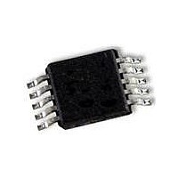
CAT5271ZI-50-GT3 ON Semiconductor, CAT5271ZI-50-GT3 Datasheet - Page 2

CAT5271ZI-50-GT3
Manufacturer Part Number
CAT5271ZI-50-GT3
Description
IC POT DPP 50K 256TAP 10MSOP
Manufacturer
ON Semiconductor
Datasheet
1.CAT5271ZI-50-GT3.pdf
(14 pages)
Specifications of CAT5271ZI-50-GT3
Package / Case
10-MSOP, Micro10™, 10-uMAX, 10-uSOP
Mounting Type
Surface Mount
Voltage - Supply
2.5 V ~ 5.5 V
Operating Temperature
-40°C ~ 85°C
Temperature Coefficient
100 ppm/°C Typical
Interface
I²C, 2-Wire Serial
Resistance In Ohms
50K
Number Of Circuits
2
Memory Type
Volatile
Taps
256
Number Of Pots
Dual
Taps Per Pot
256
Resistance
50 KOhms
Wiper Memory
Volatile
Digital Interface
I2C
Operating Supply Voltage
2.7 V to 5.5 V
Supply Current
0.3 uA
Maximum Operating Temperature
+ 85 C
Minimum Operating Temperature
- 40 C
Description/function
Dual 256-Tap Digital Potentiometer
Mounting Style
SMD/SMT
Supply Voltage (max)
5.5 V
Supply Voltage (min)
2.7 V
Tolerance
20 %
Lead Free Status / RoHS Status
Lead free / RoHS Compliant
Stresses exceeding Maximum Ratings may damage the device. Maximum Ratings are stress ratings only. Functional operation above the
Recommended Operating Conditions is not implied. Extended exposure to stresses above the Recommended Operating Conditions may affect
device reliability.
1. Maximum terminal current is bounded by the maximum current handling of the switches, maximum power dissipation of the package, and
Table 1. PIN FUNCTION DESCRIPTION
Table 2. ABSOLUTE MAXIMUM RATINGS
V
A1, B1, W1, A2, B2, W2 Voltage to GND
I
Digital Inputs and Output Voltage to GND
Operating Temperature Range
Maximum Junction Temperature (T
Storage Temperature
Lead Temperature (Soldering, 10 sec)
MAX
Pin No.
DD
maximum applied voltage across any two of the A, B, and W terminals at a given resistance.
GND
VCC
SDA
SCL
10
1
2
3
4
5
6
7
8
9
Figure 1. CAT5271 Functional Block Diagram
to GND
Pin Name
GND
VDD
SDA
SCL
W2
W1
B1
A1
A2
B2
Wiper Control
Wiper Control
Register 1
Register 2
B1 Terminal
A1 Terminal
W2 Terminal
Digital Ground
Positive Power Supply
Serial Clock Input
Serial Data Input / Output
A2 Terminal
B2 Terminal
W1 Terminal
JMAX
CAT5271
)
Rating
Description
(Note 1)
A1
W1
B1
A2
W2
B2
http://onsemi.com
2
GND
VCC
SDA
SCL
Figure 2. CAT5273 Functional Block Diagram
Pin Name
GND
VDD
AD0
SCL
SDA
AD1
W2
W1
B1
B2
AD0
Control Logic
B1 Terminal
Device Address Bit 0
W2 Terminal
Digital Ground
Positive Power Supply
Serial Clock Input
Serial Data Input / Output
Device Address Bit 1
B2 Terminal
W1 Terminal
AD1
Wiper Control
Wiper Control
CAT5273
−65 to +150
Register 1
Register 2
−0.3 to 6.5
−40 to +85
0 to 6.5
Value
V
±20
150
300
DD
Description
Unit
W1
B1
W2
B2
mA
°C
°C
°C
°C
V
V


