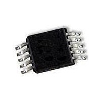
CAT5271ZI-50-GT3 ON Semiconductor, CAT5271ZI-50-GT3 Datasheet - Page 8

CAT5271ZI-50-GT3
Manufacturer Part Number
CAT5271ZI-50-GT3
Description
IC POT DPP 50K 256TAP 10MSOP
Manufacturer
ON Semiconductor
Datasheet
1.CAT5271ZI-50-GT3.pdf
(14 pages)
Specifications of CAT5271ZI-50-GT3
Package / Case
10-MSOP, Micro10™, 10-uMAX, 10-uSOP
Mounting Type
Surface Mount
Voltage - Supply
2.5 V ~ 5.5 V
Operating Temperature
-40°C ~ 85°C
Temperature Coefficient
100 ppm/°C Typical
Interface
I²C, 2-Wire Serial
Resistance In Ohms
50K
Number Of Circuits
2
Memory Type
Volatile
Taps
256
Number Of Pots
Dual
Taps Per Pot
256
Resistance
50 KOhms
Wiper Memory
Volatile
Digital Interface
I2C
Operating Supply Voltage
2.7 V to 5.5 V
Supply Current
0.3 uA
Maximum Operating Temperature
+ 85 C
Minimum Operating Temperature
- 40 C
Description/function
Dual 256-Tap Digital Potentiometer
Mounting Style
SMD/SMT
Supply Voltage (max)
5.5 V
Supply Voltage (min)
2.7 V
Tolerance
20 %
Lead Free Status / RoHS Status
Lead free / RoHS Compliant
ESD Protection
Terminal Voltage Operating Range
define the limits for proper 3−terminal digital potentiometer
operation. Signals or potentials applied to terminals A, B or
the wiper must remain inside the span of V
Signals which attempt to go outside these boundaries will be
clamped by the internal forward biased diodes.
The CAT5271/CAT5273 V
Digital
Input
W, A, B
Figure 15. ESD Protection Networks
W, A, B
LOGIC
GND
V
DD
GND
GND
Figure 16.
Potentiometer
DD
and GND power supply
LOGIC
CAT5271
DD
and GND.
http://onsemi.com
8
Power−up Sequence
compliance at terminals A, B, and W (see Figure 15), it is
recommended that V
any voltage to terminals A, B, and W. The ideal power−up
sequence is: GND, V
order of powering V
important as long as they are powered after V
Power Supply Bypassing
length layout design. Leads should be as direct as possible.
It is also recommended to bypass the power supplies with
quality low ESR Ceramic chip capacitors of 0.01 mF to
0.1 mF. Low ESR 1 mF to 10 mF tantalum or electrolytic
capacitors can also be applied at the supplies to suppress
transient disturbances and low frequency ripple. As a further
precaution digital ground should be joined remotely to the
analog ground at one point to minimize the ground bounce.
Because ESD protection diodes limit the voltage
Good design practice employs compact, minimum lead
V
Figure 17. Power Supply Bypassing
DD
10 mF
C
3
A
DD
DD
+
, V
, digital inputs, and then V
/GND be powered before applying
B
, V
0.1 mF
W
C
, and the digital inputs is not
1
V
DD
CAT5271
GND
DD
A/B/W
/GND.
. The


