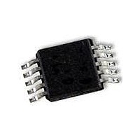
CAT5271ZI-50-GT3 ON Semiconductor, CAT5271ZI-50-GT3 Datasheet - Page 7

CAT5271ZI-50-GT3
Manufacturer Part Number
CAT5271ZI-50-GT3
Description
IC POT DPP 50K 256TAP 10MSOP
Manufacturer
ON Semiconductor
Datasheet
1.CAT5271ZI-50-GT3.pdf
(14 pages)
Specifications of CAT5271ZI-50-GT3
Package / Case
10-MSOP, Micro10™, 10-uMAX, 10-uSOP
Mounting Type
Surface Mount
Voltage - Supply
2.5 V ~ 5.5 V
Operating Temperature
-40°C ~ 85°C
Temperature Coefficient
100 ppm/°C Typical
Interface
I²C, 2-Wire Serial
Resistance In Ohms
50K
Number Of Circuits
2
Memory Type
Volatile
Taps
256
Number Of Pots
Dual
Taps Per Pot
256
Resistance
50 KOhms
Wiper Memory
Volatile
Digital Interface
I2C
Operating Supply Voltage
2.7 V to 5.5 V
Supply Current
0.3 uA
Maximum Operating Temperature
+ 85 C
Minimum Operating Temperature
- 40 C
Description/function
Dual 256-Tap Digital Potentiometer
Mounting Style
SMD/SMT
Supply Voltage (max)
5.5 V
Supply Voltage (min)
2.7 V
Tolerance
20 %
Lead Free Status / RoHS Status
Lead free / RoHS Compliant
Basic Operation
digitally controlled potentiometers. When power is first
applied, the wipers assume a mid−scale position. Once the
power supply is stable, the wipers may be repositioned via
the I
Programming: Variable Resistor
Rheostat Mode
(The following section refers to CAT5271. The behavior of
CAT5273 is identical, but for this device terminal A of the
resistor is not accessible.)
nominal value of 50 kW or 100 kW and has 256 contact
points accessed by the wiper terminal, plus the B terminal
contact. Data in the 8−bit Wiper register is decoded to select
one of these 256 possible settings.
corresponding to control position 0x00. Ideally this would
present a 0 W between the Wiper and B, but just as with a
mechanical rheostat there is a small amount of contact
resistance to be considered, there is a wiper resistance
comprised of the R
wiper output with its respective contact point. In CAT5271/
CAT5273 this ‘contact’ resistance is typically 50 W. Thus a
connection setting of 0x00 yields a minimum resistance of
50 W between terminals W and B.
point, corresponds to 441 W (R
+ 50 W) for data 0x01. The third connection is the next tap
point, is 831 W (2 x 390.6 + 50 W) for data 0x02, and so on.
Figure 14 shows a simplified equivalent circuit where the
last resistor string will not be accessed; therefore, there is
1 LSB less of the nominal resistance at full scale in addition
to the wiper resistance.
The CAT5271 and CAT5273 are dual 256−position
The resistance between terminals A and B, R
The wiper’s first connection is at the B terminal,
For a 100 kW device, the second connection, or the first tap
2
C compatible interface.
Figure 14. CAT5271 Equivalent DPP Circuit
Register
Decoder
Wiper
and
ON
of the FET switch connecting the
R
R
R
R
S
S
S
S
WB
= R
AB
/256 + R
A
W
B
W
AB
= 390.6
, has a
http://onsemi.com
7
output resistance between W and B is
where D is the decimal equivalent of the binary code loaded
in the 8−bit Wiper register, R
resistance, and R
on resistance of the internal switch.
circuited, the following output resistance R
the indicated Wiper register codes:
resistance of 50 W is still present. Current flow between W
and B in this condition should be limited to a maximum
pulsed current of no more than 20 mA. Failure to heed this
restriction can cause degradation or possible destruction of
the internal switch contact.
the DPP (Digitally Programmed Potentiometer) between the
wiper W and terminal A also produces a digitally controlled
complementary resistance R
used, the B terminal can be opened. Setting the resistance
value for R
decreases as the data loaded in the latch increases in value.
The general equation for this operation is
following output resistance R
Wiper register codes.
dependent and may vary by up to ±20%.
Table 8. CODES AND CORRESPONDING R
RESISTANCE FOR R
Table 9. CODES AND CORRESPONDING R
RESISTANCE FOR R
D (Dec.)
The equation for determining the digitally programmed
In summary, if R
Be aware that in the zero−scale position, the wiper
Similar to the mechanical potentiometer, the resistance of
For R
Typical device to device resistance matching is lot
D (Dec.)
255
128
255
128
1
0
1
0
AB
WA
= 100 kW and the B terminal open circuited, the
R
R
100,050
starts at a maximum value of resistance and
50,050
99,659
WA
WA
R
441
W
99,559
50,050
WB
R
441
(D) + 256 * D
(W)
50
is the wiper resistance contributed by the
AB
WB
(W)
= 100 kW and the A terminal is open
+ D
AB
AB
256
Full Scale
Midscale
1 LSB
Zero Scale
= 100 kW, V
= 100 kW, V
256
Full Scale (R
Midscale
1 LSB
Zero Scale
(Wiper Contact Resistance)
WA
WA
R
AB
. When these terminals are
will be set for the indicated
R
AB
) R
Output State
AB
Output State
DD
DD
) R
is the end−to−end
W
AB
= 5 V
= 5 V
WB
– 1 LSB + R
W
will be set for
WB
WA
(eq. 1)
(eq. 2)
W
)


