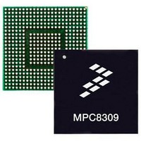
MPC8309VMAHFCA Freescale Semiconductor, MPC8309VMAHFCA Datasheet - Page 14

MPC8309VMAHFCA
Manufacturer Part Number
MPC8309VMAHFCA
Description
417/333/233 MP Std Tmp
Manufacturer
Freescale Semiconductor
Datasheet
1.MPC8309VMAHFCA.pdf
(81 pages)
Specifications of MPC8309VMAHFCA
Processor Series
MPC8309
Core
e300c3
Data Bus Width
32 bit
Data Ram Size
512 MB
Interface Type
USB, CAN, UART, PCI
Maximum Clock Frequency
417 MHz
Number Of Programmable I/os
56
Operating Supply Voltage
- 0.3 V to + 1.26 V
Maximum Operating Temperature
+ 105 C
Mounting Style
SMD/SMT
Operating Temperature Range
0 C to + 105 C
Processor To Be Evaluated
MPC8309
Supply Current (max)
5 uA
Lead Free Status / Rohs Status
Details
Available stocks
Company
Part Number
Manufacturer
Quantity
Price
Company:
Part Number:
MPC8309VMAHFCA
Manufacturer:
Freescale Semiconductor
Quantity:
10 000
Output high voltage
Output low voltage
Output low voltage
Input high voltage
Input low voltage
Input current
Note:
1. This specification applies when operating from 3.3 V supply.
DDR2 SDRAM
The following table provides the PLL lock times.
5.1
The following table provides the DC electrical characteristics for the MPC8309 reset signals mentioned in
Table
6
This section describes the DC and AC electrical specifications for the DDR2 SDRAM interface of the
MPC8309. Note that DDR2 SDRAM is GV
6.1
The following table provides the recommended operating conditions for the DDR2 SDRAM component(s)
of the MPC8309 when GV
The following table provides the DDR2 capacitance when GV
14
Input setup time for POR configuration signals
(CFG_RESET_SOURCE[0:3]) with respect to negation of PORESET
Input hold time for POR config signals with respect to negation of
HRESET
Notes:
1. t
2. POR configuration signals consist of CFG_RESET_SOURCE[0:3].
PLL lock times
II Pro Integrated Communications Processor Reference Manual.
SYS_CLK_IN
MPC8309 PowerQUICC II Pro Integrated Communications Processor Family Hardware Specifications, Rev. 1
9.
DDR2 SDRAM
Characteristic
Reset Signals DC Electrical Characteristics
DDR2 SDRAM DC Electrical Characteristics
is the clock period of the input clock applied to SYS_CLK_IN. For more details, see the MPC8309 PowerQUICC
Parameter/Condition
Table 9. RESET Initialization Timing Specifications (continued)
Table 11. Reset Signals DC Electrical Characteristics
DD
(typ) = 1.8 V
Symbol
V
V
V
V
V
I
OH
OL
IN
OL
IH
IL
Table 10. PLL Lock Times
.
DD
0 V V
I
OH
I
I
OL
(typ) = 1.8 V.
OL
Condition
= –6.0 mA
= 3.2 mA
= 6.0 mA
IN
—
—
OV
DD
Min
DD
—
(typ) = 1.8 V.
–0.3
Min
4
0
2.4
2.0
—
—
—
Max
100
OV
—
—
DD
Max
0.5
0.4
0.8
—
±5
+ 0.3
Freescale Semiconductor
t
SYS_CLK_IN
ns
Unit
s
Unit
A
V
V
V
V
V
Note
—
1, 2
1, 2
Note
—
—
1
1
1
1


