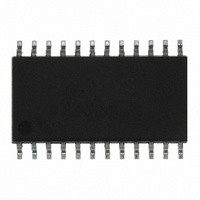
X9401WS24I Intersil, X9401WS24I Datasheet - Page 5

X9401WS24I
Manufacturer Part Number
X9401WS24I
Description
IC DCP QUAD 10K 64TP 24SOIC
Manufacturer
Intersil
Series
XDCP™r
Datasheet
1.X9401WS24ZT1.pdf
(18 pages)
Specifications of X9401WS24I
Taps
64
Resistance (ohms)
10K
Number Of Circuits
4
Temperature Coefficient
300 ppm/°C Typical
Memory Type
Non-Volatile
Interface
SPI, 3-Wire Serial
Voltage - Supply
4.5 V ~ 5.5 V
Operating Temperature
-40°C ~ 85°C
Mounting Type
Surface Mount
Package / Case
24-SOIC (7.5mm Width)
Resistance In Ohms
10K
Lead Free Status / RoHS Status
Contains lead / RoHS non-compliant
Available stocks
Company
Part Number
Manufacturer
Quantity
Price
Part Number:
X9401WS24I-2.7
Manufacturer:
INTERSIL
Quantity:
20 000
Company:
Part Number:
X9401WS24IZ-2.7T1
Manufacturer:
IDT
Quantity:
3 067
or directly between the host and the Wiper Counter Register.
These instructions are:
• Read Wiper Counter Register: read the current wiper
• Write Wiper Counter Register: change current wiper
• Read Data Register: read the contents of the selected
• Write Data Register: write a new value to the selected data
• Read Status: This command returns the contents of the
The sequence of these operations is shown in Figure 4 and
Figure 5.
The final command is Increment/Decrement. It is different
from the other commands, because it’s length is
indeterminate. Once the command is issued, the master can
clock the selected wiper up and/or down in one resistor
Detailed Potentiometer Block Diagram
IF WCR = 00[H] THEN V
IF WCR = 3F[H] THEN V
FROM INTERFACE
position of the selected pot,
position of the selected pot,
data register;
register.
WIP bit which indicates if the internal write cycle is in
progress.
(ONE OF FOUR ARRAYS)
SERIAL DATA PATH
CIRCUITRY
W
W
/R
/R
W
W
= V
= V
L
H
5
/R
/R
REGISTER 0
REGISTER 2
L
H
8
REGISTER 1
REGISTER 3
MODIFIED SCL
X9401
UP/DN
6
segment steps; thereby, providing a fine tuning capability to
the host. For each SCK clock pulse (t
the selected wiper will move one resistor segment towards
the V
while SI is LOW, the selected wiper will move one resistor
segment towards the V
the sequence and timing for this operation are shown in
Figure 6 and Figure 7.
PARALLEL
BUS
INPUT
UP/DN
CLK
SERIAL
BUS
INPUT
H
/R
REGISTER
COUNTER
H
INC/DEC
WIPER
(WCR)
LOGIC
terminal. Similarly, for each SCK clock pulse
L
C
O
U
N
E
R
T
D
E
C
O
D
E
/R
L
terminal. A detailed illustration of
HIGH
) while SI is HIGH,
October 13, 2009
V
V
V
H
L
W
/R
/R
/R
H
L
FN8190.4
W


