X9409WV24 Intersil, X9409WV24 Datasheet - Page 2
X9409WV24
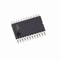
Manufacturer Part Number
X9409WV24
Description
IC DCP QUAD 10K 64TP 24TSSOP
Manufacturer
Intersil
Series
XDCP™r
Datasheet
1.X9409WS24ZT1.pdf
(20 pages)
Specifications of X9409WV24
Taps
64
Resistance (ohms)
10K
Number Of Circuits
4
Temperature Coefficient
300 ppm/°C Typical
Memory Type
Non-Volatile
Interface
I²C, 2-Wire Serial
Voltage - Supply
4.5 V ~ 5.5 V
Operating Temperature
0°C ~ 70°C
Mounting Type
Surface Mount
Package / Case
24-TSSOP
Resistance In Ohms
10K
Lead Free Status / RoHS Status
Contains lead / RoHS non-compliant
Available stocks
Company
Part Number
Manufacturer
Quantity
Price

Part Number:
X9409WV24I-2.7T1
Manufacturer:
XICOR
Quantity:
20 000
Part Number:
X9409WV24I-2.7T2
Manufacturer:
XICOR
Quantity:
20 000
Company:
Part Number:
X9409WV24IZ-2.7
Manufacturer:
STM
Quantity:
99
Part Number:
X9409WV24IZ-2.7T1
Manufacturer:
INTERSIL
Quantity:
20 000


Ordering Information
*Add "T1" suffix for tape and reel.
NOTE: Intersil Pb-free plus anneal products employ special Pb-free material sets; molding compounds/die attach materials and 100% matte tin plate
termination finish, which are RoHS compliant and compatible with both SnPb and Pb-free soldering operations. Intersil Pb-free products are MSL
classified at Pb-free peak reflow temperatures that meet or exceed the Pb-free requirements of IPC/JEDEC J STD-020.
PIN DESCRIPTIONS
Host Interface Pins
Serial Clock (SCL)
The SCL input is used to clock data into and out of the
X9409.
Serial Data (SDA)
SDA is a bidirectional pin used to transfer data into
and out of the device. It is an open drain output and
may be wire-ORed with any number of open drain or
open collector outputs. An open drain output requires
the use of a pull-up resistor. For selecting typical
values, refer to the guidelines for calculating typical
values on the bus pull-up resistors graph.
Device Address (A
The address inputs are used to set the least significant
4 bits of the 8-bit slave address. A match in the slave
address serial data stream must be made with the
address input in order to initiate communication with
the X9409. A maximum of 16 devices may occupy the
2-wire serial bus.
Potentiometer Pins
V
The V
terminal connections on either end of a mechanical
potentiometer.
X9409WS24I-2.7*
X9409WS24IZ-2.7* (Note) X9409WS ZG
X9409WV24-2.7
X9409WV24Z-2.7 (Note)
X9409WV24I-2.7*
X9409WV24IZ-2.7* (Note) X9409WV ZG
H0
/R
PART NUMBER
H0
H
/R
- V
H
H3
and V
/R
H3
L
, V
0
/R
- A
L
L0
X9409WS G
X9409WV F
X9409WV ZF
X9409WV G
PART MARKING
inputs are equivalent to the
3
/R
)
2
L0
- V
L3
/R
L3
V
CC
2.7 to 5.5
(V)
LIMITS
POTENTIOMETER
ORGANIZATION
X9409
(kΩ)
10
V
The wiper outputs are equivalent to the wiper output of
a mechanical potentiometer.
Hardware Write Protect Input (WP)
The WP pin when low prevents nonvolatile writes to
the Data Registers.
PIN NAMES
SCL
SDA
A0-A3
V
V
V
WP
V
V
NC
W0
H0
L0
W0
CC
SS
/R
/R
/R
/R
W0 -
L0
-40 to 85
-40 to 85
-40 to 85
-40 to 85
RANGE
H0
W0
0 to 70
0 to 70
Symbol
TEMP
(°C)
- V
- V
- V
V
L3
H3
W3
W3
/R
/R
24 Ld SOIC (300 mil)
/R
24 Ld SOIC (300 mil) (Pb-free)
24 Ld TSSOP (4.4mm)
24 Ld TSSOP (4.4mm) (Pb-free) MDP0044
24 Ld TSSOP (4.4mm)
24 Ld TSSOP (4.4mm) (Pb-free) MDP0044
L3
/R
H3
W3
W3
,
Serial Clock
Serial Data
Device Address
Potentiometer Pin
(terminal equivalent)
Potentiometer Pin
(wiper equivalent)
Hardware Write Protection
System Supply Voltage
System Ground (Digital)
No Connection
PACKAGE
Description
October 12, 2006
M24.3
MDP0027
MDP0044
MDP0044
DWG. #
PKG.
FN8192.4
Related parts for X9409WV24
Image
Part Number
Description
Manufacturer
Datasheet
Request
R

Part Number:
Description:
Intersil Corporation [CMOS Serial Controller Interface]
Manufacturer:
Intersil Corporation
Datasheet:
Part Number:
Description:
Manufacturer:
Intersil Corporation
Datasheet:
Part Number:
Description:
357-036-542-201 CARDEDGE 36POS DL .156 BLK LOPRO
Manufacturer:
Intersil Corporation
Datasheet:
Part Number:
Description:
1024-Word x 4-Bit LSI Static RAM
Manufacturer:
Intersil Corporation
Datasheet:
Part Number:
Description:
General Purpose NPN Transistor Arrays FN341.4
Manufacturer:
Intersil Corporation
Datasheet:
Part Number:
Description:
CMOS 16-Bit Microprocessor
Manufacturer:
Intersil Corporation
Datasheet:
Part Number:
Description:
Manufacturer:
Intersil Corporation
Datasheet:
Part Number:
Description:
Manufacturer:
Intersil Corporation
Datasheet:
Part Number:
Description:
Manufacturer:
Intersil Corporation
Datasheet:
Part Number:
Description:
Manufacturer:
Intersil Corporation
Datasheet:
Part Number:
Description:
CMOS 6-Bit Latch and Decoder Memory Interfaces
Manufacturer:
Intersil Corporation
Datasheet:
Part Number:
Description:
CA3046General Purpose NPN Transistor Arrays
Manufacturer:
Intersil Corporation
Datasheet:
Part Number:
Description:
Manufacturer:
Intersil Corporation
Datasheet:
Part Number:
Description:
TR909 DLC/FLC SLIC with Low Power Standby
Manufacturer:
Intersil Corporation
Datasheet:
Part Number:
Description:
Manufacturer:
Intersil Corporation
Datasheet: